Overview
The consumer electronics industry depends a lot on device reliability. Simulation and testing are two tools that let designers make sure a product works well. Good design must predict the needs of the full PCB and provide what is needed to meet those needs. Solid DFT, DFM, and DFA design practices are vital to make a board that can be made and used reliably.
Designers must add test points and other test features to the PCB so technicians can run checks during the test stage. A good design must also meet the rules that make board manufacture and assembly easy. Spending time on the schematic and simulation early can cut development time and make the final product more reliable.
Design for Test (DFT)
Testing and inspection are essential steps in the PCB product cycle. DFT means adding items such as test points to the PCB to make it easier to test the circuit’s function. Extra test points help engineers check the board after it is built. The goal is to find and confirm any manufacturing flaws that might stop the product from working.
Key DFT Ideas
Two key ideas in DFT are controllability and observability:
- Controllability: The ability to set certain circuit nodes or inputs to a known state or logic value.
- Observability: The ability to see the state or logic value of internal nodes or outputs.
These two ideas let engineers put the design into a known start state and then control and watch internal signals. This helps check whether the device works as it should. Tests can then spot functional faults or manufacturing defects.
Common Functional Faults and Checks
- A functional fault refers to incorrect or poor output from the system, caused by poor circuit behavior or repeated functional errors.
- Errors may be fixed with code adjustments or minor modifications, but serious faults indicate the need for design changes.
- The process of detailed fault diagnosis is called Failure Mode Analysis (FMA).
- During functional testing, engineers also verify routed currents, pin voltages, power levels, switching and timing signals, and board temperature.
Common Manufacturing Defects
Manufacturing defects stem from issues such as excess metal residue on the board, poor plating, contamination in solder joints, and dielectric problems. These can lead to short circuits, open circuits, weak solder joints, or insulation failure. It is crucial to design to minimize the risk of such defects and facilitate their detection if they occur.
Two Ways to Add DFT Features
1. Temporary Technique
- Adds test features without major changes to the original design.
- Uses temporary test points to test the device without adding numerous permanent test pads.
- Advantages: Cost-effective, quick to implement, suitable for early production runs and prototypes.
2. Structural Technique
- A permanent solution that integrates dedicated test points into the board design.
- Advantages: Simplifies debugging; if a defect occurs, permanent test points make it easier to locate and fix issues.
- Best for large-scale detection of manufacturing defects.
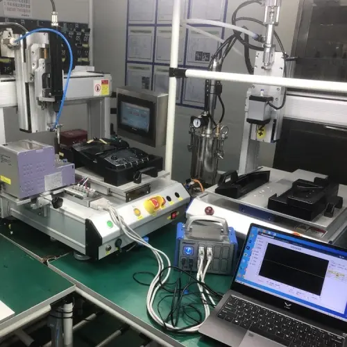
ICT — In-Circuit Test
- ICT (In-Circuit Test) typically uses a bed-of-nails fixture.
- Functions: Measures resistance, capacitance, and other passive component values; verifies the functionality of analog components (e.g., amplifiers, oscillators); detects common issues like short circuits, open circuits, or incorrect components.
- Typical setup: Includes a tester, a fixture, and test software.
Flying Probe Test
- A simple and effective form of ICT.
- Key features: Probes can move freely on the PCB to touch required test points; no fixed fixture required, making it cost-effective for small-batch production or prototypes.
- Advantage: For design changes, test points do not require hardware modifications—only updates to the test program are needed.
Design for Manufacturability (DFM)
Component availability and manufacturing methods vary by company and country. Electromagnetic Compatibility (EMC) is another mandatory standard for devices before they can be marketed. Designers must ensure the design aligns with available manufacturing processes, usable components can fulfill required functions, and the final layout meets specified size and shape requirements. DFM (Design for Manufacturability) involves planning and designing a product to enable easy and low-cost manufacturing.
DFM Goals
DFM helps accelerate PCB production, reduce production time and costs. Below are key checks and best practices for DFM:
1. Component Selection
- Standard components are more reliable and cost-effective than custom components, adding value to the product.
- Using standard components simplifies logistics: replacement is easier in case of failure compared to custom components.
- Standard components typically have clear tolerances and good solderability.
2. Board Form and Layout
- Adhere to customer-specified shape and size requirements.
- Consider connector placement and group circuits by power, frequency, and routing needs.
- Place functionally related components close to minimize trace length and interference.
3. Minimize Part Count
- Reducing the number of components lowers costs and simplifies manufacturing, potentially reducing the number of PCB layers.
- Determine the number of layers based on board area, power routing, signal integrity, isolation requirements, and the number of high-speed signals.
4. Reuse Design Elements
- Design reusable components to cut costs (e.g., a well-designed ground plane can serve as a structural layer, EMI shield, and signal integrity enhancer).
- Comply with DFM rules: minimum trace width, trace-to-trace spacing, and correct via annular ring size.
5. Compliance and EMC
- Plan EMC and power usage compliance from the initial design stage to improve product quality and reduce costly rework.
- Allow tolerance for minor post-manufacturing changes in board size or component placement to avoid assembly or performance errors.
6. Handling and Packaging
- Avoid asymmetric designs, which may cause damage during handling (leading to failures).
- Minimize use of fragile or overly flexible parts.
- Use secure, compact packaging to protect the board during shipping and use.
Design for Assembly (DFA)
The electronics industry relies on the ease of component assembly. Devices are manufactured by sourcing local and global parts and assembling them as required. Fewer parts reduce assembly time; modules designed for ease of assembly streamline the entire process. DFA (Design for Assembly) is a design approach that prioritizes assembly ease, delivering significant cost savings.
DFA Best Practices
1. Reduce Part Variety
- Use the same component across multiple locations to reduce inventory, simplify pick-and-place operations, and minimize errors.
2. Make Parts Easy to Place
- Select components with clear polarity markers for easy orientation.
- Design footprints that match actual component dimensions and provide sufficient pad area for reliable soldering.
3. Group Parts Logically
- Cluster components requiring testing or tuning.
- Group parts by function to enable orderly assembly and testing.
4. Design for Automated Assembly
- Ensure layout compatibility with pick-and-place machines and reflow ovens for automated production lines.
- Keep the board flat and avoid tall components that may obstruct the assembly of adjacent parts.
5. Allow Manual Work
- Reserve space for workers to access pads and connectors for manual assembly steps.
- Use fiducials and clear markers for alignment by equipment and personnel.
6. Use Good Mechanical Design
- Design board shape and mounting holes for easy installation in enclosures.
- Provide clear mounting points and avoid designs that cause board stress during installation.
Practical Checks and Examples
1. Trace Width and Spacing
- Follow the PCB manufacturer’s minimum requirements for trace width and spacing.
- Wider traces carry more current and are easier to manufacture; sufficient spacing between traces reduces short-circuit risks.
2. Via Design
- Select appropriate via size and annular ring. Small vias save space but are harder to plate and may be less reliable—balance size and performance.
3. Solder Mask and Silkscreen
- Use solder mask to prevent shorts and facilitate soldering.
- Keep silkscreen clear and away from pads to avoid printing on solderable areas.
4. Thermal and Power Planning
- Allocate adequate copper area for power components to dissipate heat.
- Use thermal reliefs on pads where necessary; place power components to avoid heat buildup near sensitive parts.
5. EMI and Grounding
- Use solid ground planes and short return paths.
- Keep high-speed traces short and controlled for impedance.
- Place bypass capacitors close to power pins and route power nets carefully.
6. Assembly Test Points
- Position test pads for easy probe access, free from obstruction by other components.
- Use standard-sized test pads to prevent damage during probing.
7. Packaging and Shipping
- Use anti-static padding to protect the board.
- Package boards to prevent bending or contact between units; protect exposed connectors and fragile components.
Conclusion
In the PCB production cycle, approximately 70% of manufacturing costs are determined during the early design stage. Implementing DFM from the start reduces costs and accelerates time-to-market. DFT ensures post-manufacturing functionality, while DFA lowers assembly time and expenses. By following best practices for DFT, DFM, and DFA, designers can create reliable, cost-effective PCBs.
Simple Checklist (for Quick Review)
- Add test points for key nets.
- Ensure nets are controllable and observable.
- Prioritize standard components where possible.
- Minimize part count and layer count.
- Comply with vendor specifications for trace width and spacing.
- Use ground planes and place bypass capacitors near power pins.
- Design footprints matching actual component dimensions.
- Reserve space for test probes and pick-and-place tools.
- Plan for handling, packaging, and mounting.
- Conduct ICT or flying probe tests on prototypes.