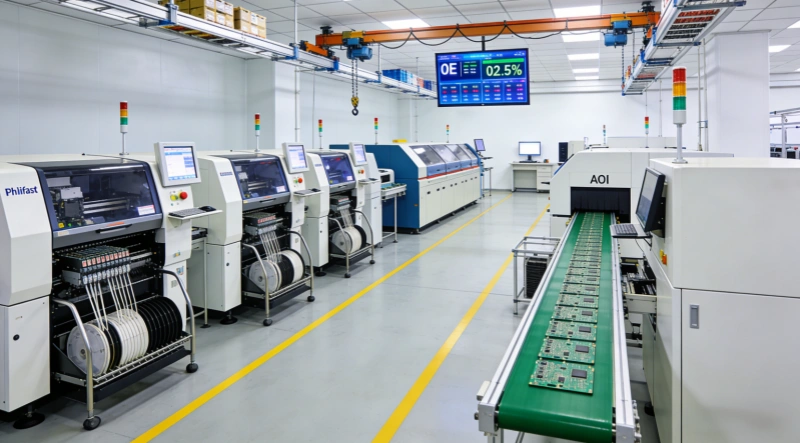
SMT has emerged as a cornerstone, enabling the production of compact, efficient, and high-performance electronic devices. For companies like Philifast electronics manufacturing, their SMT production line represents the perfect blend of cutting-edge technology, rigorous quality control, and efficient workflow. Through Philifast’s SMT process, from the initial component loading to the final Automated Optical Inspection (AOI), uncovering the engineering precision and operational excellence that define their output. SMT manufacturing turns design into reliable, high-quality PCBs.
Philifast’s SMT line is designed to handle volumes from prototyping to mass production, with a focus on flexibility and quality. Every machine, process, and team member is aligned to meet strict industry standards and deliver PCBs with near-zero defect rates. Now, let’s dive into the step-by-step journey of a PCB through.
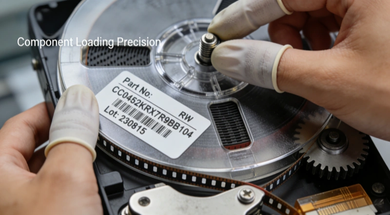
Stage 1: Component Preparation & Loading: The Foundation of Precision
At the component loading station, where the raw materials for electronic assembly are prepared. Components such as resistors, capacitors, integrated circuits (ICs), and other surface-mount devices (SMDs) are carefully loaded into reels or trays. There storage solution are designed to feed components accurately and consistently into the SMT machines.
Components are loaded onto tape and reel carriers, standardized packaging the that allows for automated feeding into SMT machines. Philifast’s operators use precision tools to load reels onto feeders, which are then mounted on the pick-and-place machines. Each feeder is calibrated to match the component’s size and pitch (distance between components on the reel), ensuring accurate pickup.
PCB Preparation
While components are being prepared, PCBs are cleaned to remove dust, oil, or debris that could interfere with solder paste adhesion. The PCBs are then loaded onto pallets or conveyor belts, ready to enter the solder paste printing station. Each PCB is inspected for defects (e.g., scratches, bent pads) before proceeding—any faulty boards are flagged and removed to avoid wasted production time.
Stage 2: Solder Paste Printing: The Foundation of SMT
Once the components are loaded, the printed circuit boards (PCBs) enter the solder paste application stage. Solder paste, a mixture of tiny solder spheres and flux, is applied to the PCB pads through a stencil using a solder paste printer. This process ensures that each pad receives the precise amount of solder paste required for component attachment.
The quality of solder paste application directly impacts the solder joint integrity and, consequently, the reliability of the electronic device. Philifast utilizes advanced solder paste inspection systems to verify the accuracy and uniformity of solder paste deposition, minimizing the risk of solder-related defects.
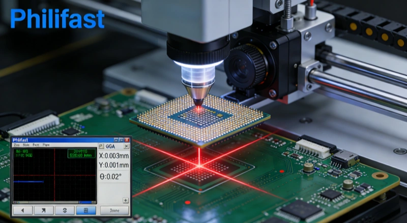
Stage 3: Pick and Place – Robotics & Precision at Scale
After solder paste printing, the PCB moves to the pick-and-place station, the most automated and fastest stage of the SMT process. Philifast uses a combination of high-speed pick and place machines and precision placement robots to mount components onto the PCB with micron-level accuracy.
Machine Setup
Each pick-and-place machine is programmed using the PCB’s CAD file, which maps the exact location of every component. The machine’s feeders (loaded with tape-and-reel components) are aligned to the program, and the robot’s nozzles are selected based on component size—small nozzles for 01005 chips (the smallest standard SMT components) and larger nozzles for ICs or connectors.
Component Placement
The pick-and-place robot uses optical recognition to identify components on the feeder, pick them up with vacuum nozzles, and place them precisely onto the solder paste-covered pads. High-speed machines can place up to 50,000 components per hour, while precision machines handle larger, more sensitive components (e.g., BGA chips) with slower, more controlled movements.
Philifast’s line includes multiple pick-and-place machines working in tandem—some focused on small passive components (resistors, capacitors) and others on active components (ICs, sensors). This division of labor maximizes speed without compromising accuracy.
Post-Placement Verification
After placement, a vision system checks that all components are correctly positioned, no missing parts, no misalignment, no flipped components. If a component is misplaced, the machine flags the PCB for manual inspection. This step ensures that components are ready for soldering and reduces the risk of defects during reflow.
Stage 4: Reflow Soldering – Melting the Paste to Create Permanent Bonds
Once all components are placed, the PCB enters the reflow oven, where the solder paste is melted (reflowed) to create permanent electrical and mechanical bonds between components and the PCB. Philifast uses convection reflow ovens, the most advanced type—for uniform heating and precise temperature control.
The reflow process follows a carefully calibrated temperature profile with four stages:
- Preheat: The PCB is heated gradually (1–3°C per second) to 150–180°C to evaporate moisture and activate flux in the solder paste (flux cleans the pads and components to improve solder adhesion).
- Soak: The temperature is held steady for 60–90 seconds to ensure all components reach the same temperature, preventing thermal shock.
- Reflow: The temperature rises rapidly to 217–225°C (above the solder paste’s melting point of ~183°C), melting the solder and forming joints.
- Cooling: The PCB is cooled quickly (2–4°C per second) to solidify the solder, creating strong, reliable joints.
Philifast’s engineers adjust the profile based on the PCB’s size, component density, and type of solder paste (lead-based or lead-free).
Post-Reflow Inspection
After cooling, the PCB undergoes a visual inspection to check for soldering defects, such as:
- Bridging: Solder connecting two adjacent pads (a common issue with fine-pitch components).
- Tombstoning: Components standing upright due to uneven solder paste application.
- Cold joints: Dull, grainy solder joints caused by insufficient heating.
Operators use magnifying glasses or digital microscopes for manual inspections, while automated systems check high-volume runs. Defective PCBs are sent to the rework station for repair.
Stage 5: AOI Inspection and Quality Control – Ensure Perfection
Following reflow soldering, the PCBs undergo a series of inspections to verify the quality and integrity of the solder joints and component placement. The first line of inspection is typically a manual visual inspection, where trained technicians visually inspect the PCBs for any obvious defects or anomalies.
However, manual inspection is time-consuming and prone to human error. To enhance inspection accuracy and efficiency, Philifast employs Automated Optical Inspection (AOI) systems. AOI machines use high-resolution cameras and advanced image processing algorithms to detect defects such as misaligned components, insufficient solder, solder bridges, and other anomalies that may not be visible to the naked eye. AOI is the final safeguard before PCBs are shipped to clients, ensuring only flawless products leave the facility.
How AOI Works
AOI machines capture high-resolution images of the PCB from multiple angles, comparing them to a “golden sample” (a perfect PCB) stored in the system. The AI-powered software analyzes the images to identify defects such as missing components, misaligned parts, soldering issues, and even tiny scratches on the PCB surface.
Philifast uses 2D AOI machines: Ideal for checking component presence, alignment, and basic soldering defects.
AOI systems classify defects by severity (critical, major, minor) and flag them for review. Critical defects (e.g., missing IC chips, short circuits) require immediate rework or disposal, while minor defects (e.g., tiny solder splatters) are documented but may be acceptable based on client specifications. Philifast’s quality team reviews all AOI reports, and the data is used to optimize earlier stages of the process (e.g., adjusting solder paste printing parameters to reduce bridging).
Beyond Production: Philifast’s Commitment to Quality & Innovation
Philifast’s SMT line is more than just a series of machines—it’s a system built around continuous improvement and client satisfaction. Here’s what sets their process apart:
Traceability
Every PCB is assigned a unique serial number, allowing Philifast to trace every component, machine, and operator involved in its production. This traceability is critical for industries like aerospace and medical devices, where compliance with regulatory standards is mandatory.
Flexibility
The line is designed to handle both low-volume prototyping and high-volume mass production. Quick changeovers allow Philifast to switch between different PCB designs, making them ideal for clients with diverse or evolving needs.
Sustainability
Philifast prioritizes eco-friendly manufacturing, using lead-free solder paste, energy-efficient machines, and recycling programs for waste materials. Their reflow ovens and AOI systems are calibrated to minimize energy consumption, reducing the line’s carbon footprint.
Conclusion
From component loading to AOI inspection, Philifast’s SMT production line exemplifies the precision, efficiency, and quality that modern electronics manufacturing demands. By combining cutting-edge technology (AOI, high-speed pick-and-place robots) with rigorous quality control (PPI, post-reflow inspection, traceability), they deliver PCBs that meet the most demanding industry standards.
Whether you’re looking for prototyping services or mass production of high-reliability PCBs, Philifast’s SMT line is equipped to handle your needs. Their commitment to innovation and client satisfaction ensures that every product is not just built to spec—but built to last.
If you’re interested in learning more about Philifast’s SMT capabilities or partnering with them for your next project, visit our website at https://flj-pcb.com/ or contact sales team for a custom quote.
FAQ:Frequently Asked Questions About Philifast’s SMT Production Line
Q1: What types of PCB volumes can Philifast’s SMT line handle?
A1: Philifast’s SMT production line is designed for full flexibility, covering both low-volume prototyping and high-volume mass production needs. With quick changeover times, the line can easily switch between different PCB designs, making it suitable for clients with diverse or evolving project requirements, from small-batch prototype development to large scale commercial production runs.
Q2: Does Philifast use lead-free solder, and is it compliant with industry standards?
A2: Yes, Philifast prioritizes eco-friendly manufacturing and uses lead-free solder paste as standard. Additionally, the entire SMT process adheres to strict industry standards, including IPC-A-610. This compliance ensures that PCBs meet the reliability and quality requirements for industries such as consumer electronics, aerospace, and medical devices.
Q3: What happens if a defect is detected during the SMT process?
A3: Defects are addressed at multiple checkpoints throughout the SMT process to minimize waste and ensure quality. If a defect is detected (e.g., misaligned components during post-placement verification, soldering issues during post-reflow inspection, or anomalies in AOI), the PCB is flagged for review. Critical defects (e.g., missing IC chips, short circuits) require immediate rework or disposal, while minor defects are documented and assessed against client specifications. All defect data is also used to optimize earlier production stages (e.g., adjusting solder paste printing parameters to reduce bridging) for continuous improvement.