1. Core Principles of Stackup Design
Overall, stackup design must follow two rules:
- Each routing layer must have a nearby reference layer. The reference layer can be a power plane or a ground plane.
- Keep the main power plane and ground plane as close as possible. This gives a larger coupling capacitance.
Below are example stackups from two-layer boards up to eight-layer boards.
2. Stackup Schemes by PCB Layer Count
2.1 One- and Two-Layer Board Stackups
For two-layer boards, the layer count is low. Stackup issues do not exist the same way they do for many-layer boards. Control of EMI radiation must come from routing and layout.
Single-layer and double-layer boards have growing EMC problems. The main cause is that signal loop areas can become large. Large loop areas not only make strong radiation, they also make the circuit sensitive to outside noise. To improve EMC, the simplest step is to reduce the loop area of key signals.
Key signals: From the EMC view, key signals are those that make strong radiation and those that are sensitive to outside noise. Signals that make strong radiation are usually periodic signals. These include clocks and low-order address signals. Signals that are sensitive to noise are usually low-level analog signals.
Single- and double-layer boards are usually used in low-frequency analog designs below 10 kHz. Use these basic rules:
- Route power on the same layer in a radial way when you can. Try to keep the total length of traces small.
- Keep power and ground traces close to each other. Place a ground trace next to a key signal. Put that ground trace as close to the signal as you can. This creates a small loop area. Small loop area lowers common-mode radiation and reduces how sensitive the signal is to outside noise. When you put a ground trace beside the signal, the small loop will attract the signal return current. The signal current then goes through this small loop and not through other ground paths.
- For a double-sided board, place a wide ground trace on the other side of the board right under the signal trace. Make this ground trace as wide as possible. This makes a loop area that equals board thickness times the signal length.
2.2 Four-Layer Board Stackups
Common four-layer stackups include:
- SIG – GND (or PWR) – PWR (or GND) – SIG
- GND – SIG (or PWR) – SIG (or PWR) – GND
For both of these stackups, there is a potential problem with a standard board thickness of 1.6 mm (62 mil). The spacing between layers becomes large. Large spacing makes it hard to control impedance, layer coupling, and shielding. In particular, if the spacing between power and ground planes is large, the board capacitance drops. Low board capacitance is not good for filtering noise.
For the first stackup (SIG – GND/PWR – PWR/GND – SIG)
People often use it when there are many chips on the board. This stackup gives good signal integrity. EMI performance is not as good. You must control EMI by careful routing and other details.
Key points:
- Put the ground plane next to the signal layer that has the most dense routing. This helps absorb and reduce radiation.
- Also increase board area. Follow the 20H rule.
For the second stackup (GND – SIG/PWR – SIG/PWR – GND)
People use it when chip density is low and when the chip area has space for power copper pours. In this design, the outer layers are ground planes and the two inner layers are signal or power. Route power on the signal layer with wide traces. Wide traces make the power path impedance low and the microstrip signal impedance low. The outer ground layers can shield inner signals from radiating. From an EMI control view, this is the best four-layer PCB structure available now.
Key points:
- Keep the spacing between the two inner mixed signal and power layers larger.
- Make the routing directions orthogonal between those layers to avoid crosstalk.
- Control board area and follow the 20H rule.
- If you must control routing impedance, place traces carefully under the power and ground copper islands.
- Also, try to interconnect copper pours on the power or ground layers as much as possible. This gives good DC and low-frequency connectivity.
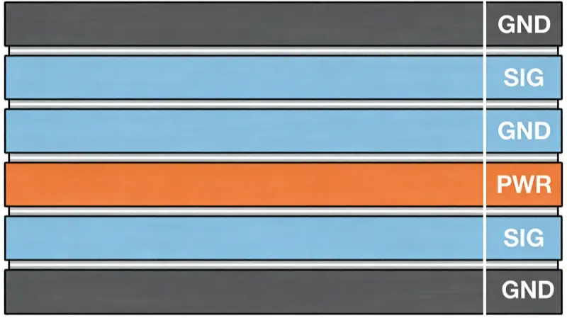
2.3 Six-Layer Board Stackups
For designs with high chip density and high clock speed, consider six-layer boards. Two recommended six-layer stackups are as follows:
Option 1: SIG – GND – SIG – PWR – GND – SIG
With this scheme, you get good signal integrity. Each signal layer sits next to a ground plane. The power and ground planes are paired. You can control the impedance of each routing layer well. Both ground planes can absorb magnetic flux well. With full power and ground planes, each signal layer has a good return path.
Option 2: GND – SIG – GND – PWR – SIG – GND
This option fits boards where device density is not very high. It keeps the advantages of the first option. Also, the top and bottom ground planes are more continuous. They act as good shields.
Note: Put the power plane near the side that is not the main component face. The bottom plane will be more complete then, and EMI performance will be better than the first option.
Summary for six-layer boards:
Keep the distance between power and ground planes as small as possible. This gives good power-ground coupling. On a 62 mil board thickness, the layer spacing is smaller than four-layer options. Still, it is not easy to make the main power and ground spacing very small. Compared to the second option, the first option costs less. So we often choose the first form for practical stackup. Follow the 20H rule and the mirror layer rule in design.
2.4 Eight-Layer Board Stackups
Eight-layer boards have many possible stackups. Some are worse for EMI because of poor absorption and large power impedance. Here are three forms described:
Type A (not good)
This form has lower electromagnetic absorption and larger power impedance. Its layer order is:
- Signal 1: component side, microstrip routing layer
- Signal 2: inner microstrip routing layer, good routing layer (X direction)
- Ground
- Signal 3: stripline routing layer, good routing layer (Y direction)
- Signal 4: stripline routing layer
- Power
- Signal 5: inner microstrip routing layer
- Signal 6: microstrip routing layer
This form is not a good choice because it does not provide consistent references for all signal layers. Power impedance is high and EMI control is weak.
Type B (variant with added reference layers)
This is a variant of a third type. By adding reference layers it gets better EMI performance. The characteristic impedance of each signal layer can be well controlled. One possible order is:
- Signal 1: component side, microstrip routing layer, good routing layer
- Ground: good wave absorption
- Signal 2: stripline routing layer, good routing layer
- Power: this power plane and the ground below it form good electromagnetic absorption
- Ground: ground plane
- Signal 3: stripline routing layer, good routing layer
- Power: this power plane has larger power impedance
- Signal 4: microstrip routing layer, good routing layer
Type C (best practice)
This is the best stackup form. It uses multiple ground reference planes. This gives very good electromagnetic absorption. A common order is:
- Signal 1: component side, microstrip routing layer, good routing layer
- Ground: good wave absorption
- Signal 2: stripline routing layer, good routing layer
- Power: this power plane and the ground below it form excellent electromagnetic absorption
- Ground: ground plane
- Signal 3: stripline routing layer, good routing layer
- Ground: second ground plane, good wave absorption
- Signal 4: microstrip routing layer, good routing layer
3. How to Choose Layer Count and Stackup
Choose the number of layers and the stackup form based on many factors. These include: the number of signal nets on the board, component density, pin density, signal frequencies, and board size. Consider all of these together.
Design notes:
- If there are many signal nets, design with more layers.
- If component density is high, choose more layers.
- If pin density is high, choose more layers.
- If signal frequency is high, choose more layers.
- To get good EMI performance, try to make sure every signal layer has its own reference layer. A reference layer can be ground or power. This helps control impedance and gives tight return paths. Tight return paths lower loop area. Lower loop area reduces radiation and sensitivity to interference.
4. Simple Rules to Follow in All Designs
- Give each routing layer a nearby reference plane. This helps control impedance and return current.
- Pair power and ground planes when you can. Keep the spacing small. This increases plane capacitance. High plane capacitance lowers noise.
- Put the ground plane next to the signal layer that has dense routing. This helps absorb and stop radiation.
- Use orthogonal routing on adjacent signal layers to lower crosstalk.
- Use wide traces for power routing on mixed layers to keep power path impedance low.
- Interconnect copper pours on power and ground planes to get strong DC and low-frequency connections.
- Follow the 20H rule when you set board area and keep mirror layer design rules in mind.
- In high speed or high density designs, prefer six-layer or eight-layer boards so each signal layer can have a close reference.
- For low frequency analog designs, one- or two-layer boards can work if you keep loop areas small and place ground near signals.
- When you can, make inner power and ground planes close. This improves decoupling and reduces EMI.
5. Closing Note
Stackup choice is a system trade. Look at nets, layout, component placement, pin count, and frequency all at once. For better EMI and signal control, give each signal layer a clear nearby reference. Use paired planes and narrow plane spacing when possible. Use multiple ground planes for best electromagnetic absorption in many-layer boards. When you design, balance cost and performance. Follow the simple rules above and choose the stackup that fits your board needs.