A via is one of the key parts of a multi-layer printed circuit board (PCB). In many boards, drilling costs make up about 30% to 40% of the board fabrication cost. In simple words, any hole on a PCB can be called a via. From its role, a via has two main uses: one is to make electrical connections between layers, and the other is to fix or locate parts.
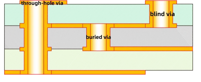
If we look at the manufacturing process, vias can be grouped into three types: blind via, buried via, and through via (through-hole via). A blind via starts from the top or bottom surface of the PCB and goes down to some inner layer. It has a certain depth and is used to link surface traces to inner layer traces. The depth of a blind via usually does not exceed a certain ratio relative to the hole diameter. A buried via is a hole that connects inner layers only; it does not reach any surface of the board. Both blind and buried vias are made inside the board before lamination, and they may overlap several inner layers during their formation. The third type is the through via. This hole goes all the way through the board. It can be used for internal interconnections or as a mounting or locating hole for parts. Because through vias are easier to make and cheaper, most printed circuit boards use them instead of blind or buried vias. In the rest of this text, unless we say otherwise, the word “via” refers to a through via.
Via structure and why size matters
From a design point of view, a via has two main parts. One is the center drill hole. The other is the pad area around the drilled hole. The sizes of these two parts determine the via size. When a PCB needs high speed and high density, designers want vias to be as small as possible. Small vias leave more room for routing on the board. Also, smaller vias have lower parasitic capacitance, so they suit high-speed circuits better.
But making vias smaller increases cost. Also, via size cannot be reduced without limit. The limit comes from the drill and plating processes. The smaller the hole, the longer drilling takes, and the more the drill can wander off center. Also, when the hole depth is more than six times the drill diameter, it is hard to ensure the hole wall gets an even copper plating. For example, a normal six-layer PCB has a thickness (via depth) of about 50 mil. Under that condition, the PCB factory can usually drill down to a minimum diameter of around 8 mil.
Parasitic capacitance of a via
A via has parasitic capacitance to ground. If we know the diameter of the ground clearance hole on the plane layer is D2, the via pad diameter is D1, the PCB board thickness is T, and the board substrate dielectric constant is ε, then the approximate parasitic capacitance of the via is:
C = 1.41 × ε × T × D1 / (D2 − D1)
This formula gives a reasonable estimate for the via capacitance. The parasitic capacitance mainly makes the signal rise time longer and so lowers circuit speed.
Let us use a concrete example. Suppose the board thickness is 50 mil. The via inner diameter is 10 mil and the pad diameter is 20 mil. The distance between the pad and the ground copper area is 32 mil. Using the formula above and taking ε = 4.4, we get:
C = 1.41 × 4.4 × 0.050 × 0.020 / (0.032 − 0.020) ≈ 0.517 pF
This amount of capacitance changes the rise time. If the characteristic impedance is 55 ohms, the change in the 10%–90% rise time caused by this capacitance is approximately:
T10−90 = 2.2 × C × (Z0 / 2) ≈ 2.2 × 0.517 × (55 / 2) ≈ 31.28 ps
From these numbers we see that a single via’s parasitic capacitance has only a small effect on rise time. But if a signal crosses many vias when changing layers, the effect will add up. Then the designer must think carefully about it.
Parasitic inductance of a via
Along with parasitic capacitance, a via also has parasitic inductance. In high-speed digital design, the harm from the via’s parasitic inductance is often greater than that from parasitic capacitance. The via’s series inductance can weaken the effect of bypass capacitors and reduce the filtering performance of the whole power system.
A simple approximate formula for the via inductance is:
L = 5.08 × h × [ ln(4h / d) + 1 ]
where:
- L is the via inductance,
- h is the via length,
- d is the center drill diameter.
From the formula we see that the via diameter has a small effect on inductance, and the via length has the largest effect. Using the example above with h = 0.050 and d = 0.010, we get:
L = 5.08 × 0.050 × [ ln(4 × 0.050 / 0.010) + 1 ] ≈ 1.015 nH
If the signal rise time is 1 ns, the equivalent inductive reactance is:
XL = π × L / T10−90 ≈ π × 1.015 nH / 1 ns ≈ 3.19 Ω
When there is high frequency current, an impedance of this level cannot be ignored. Note also that a bypass capacitor placed to connect the power layer and ground layer usually needs two vias. That means the via inductance will be doubled for this bypass path.
What this means for high-speed design
From the above analysis of via parasitics, we can see that a seemingly simple via can cause big negative effects in a high-speed PCB. To reduce these problems, designers can try the following measures.
- Choose a reasonable via size
Think about both cost and signal quality. For example, for memory module PCBs with 6 to 10 layers, choosing a 10/20 mil (drill/pad) via works well. For some high-density, small boards, you may try 8/18 mil vias. Under current technology, it is hard to make vias smaller than that. For power or ground vias, use larger sizes to lower impedance. - Use a thinner board if possible
As the formulas show, a thinner board helps reduce both via capacitance and inductance. - Avoid unnecessary layer changes
Try to route signals without switching layers. In other words, use as few vias as possible. - Place power and ground pins near vias
Put power and ground pins close to their vias. Keep the lines between the via and the pin as short as possible, because long lines increase inductance. Use thicker traces for power and ground to lower impedance. - Place ground vias near signal layer-change vias
Put ground vias near vias where signals change layers. This gives the signal a nearby return path. You can also add many extra ground vias if needed. But be flexible. The via model discussed earlier assumed a pad at every layer. In some cases you can reduce or remove pads on some internal layers. When via density is very high, large pads on a copper pour can form a broken loop. To fix this you can move some vias or reduce pad sizes on certain layers.
Via design for high-speed PCBs — practical suggestions
High-speed PCBs usually use multiple layers, and vias are a major factor in the design. A via in a PCB has three parts: the hole itself, the pad around the hole, and the power-layer isolation zone (the clearance on power and ground planes around the via).
Here are some practical points for high-speed multi-layer boards:
- Via size recommendations
For general multi-layer boards with moderate density, a via with dimensions 0.25 mm / 0.51 mm / 0.91 mm (drill / pad / power isolation) is a good choice. For high-density boards, 0.20 mm / 0.46 mm / 0.86 mm may work. Non-plated vias can be used in some designs. For power or ground vias, consider larger sizes to lower impedance. - Power isolation zone
The larger the power isolation area, the better. Consider the via density on the plane. Often D1 = D2 + 0.41 is used as a guideline, meaning the pad diameter equals the plane clearance diameter plus 0.41 mm. This helps keep plane clearance wide enough. - Minimize layer changes
Reduce vias by avoiding unnecessary layer changes in signal routing. - Use thinner boards
Thinner boards lower both capacitance and inductance of vias. - Short and wide power/ground connections
Keep the lead from via to power or ground pin short. Make the traces as wide as practical for power or ground to reduce inductive impedance. - Ground via stitching near layer-change vias
Add ground vias close to vias where a signal moves between layers. This gives the signal a short return path.
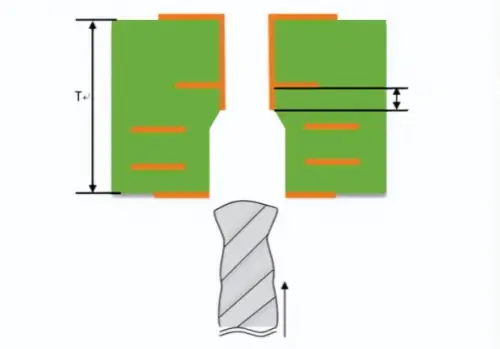
Also note via length is a main factor for via inductance. For top and bottom layer through vias, the via length equals the full board thickness. As layer counts increase, board thickness may exceed 5 mm. In high-speed design, via length is usually kept below 2.0 mm to reduce via-related problems. For via lengths greater than 2.0 mm, increasing the via diameter can help restore impedance continuity. When the via length is 1.0 mm or less, the best via diameter is about 0.20 mm to 0.30 mm.
Backdrilling in PCB production
1. What is backdrilling?
Backdrilling is a special drill step used on deep-hole boards. For example, in making a 12-layer board we might want to connect layer 1 to layer 9. Normally we drill a through-hole once and then plate. That via then runs from layer 1 to layer 12, but we only need a connection between layer 1 and layer 9. The extra section from layer 10 to layer 12 acts like a stub. This stub affects signal paths and can cause signal integrity problems in communication signals. To remove this extra stub, we drill it out from the back side — a second drilling step. This is called backdrilling. In practice, manufacturers do not drill out every last bit, because later steps remove some copper and the drill bit has a tapered tip. So the factory usually leaves a very small stub. The leftover stub length is called the B value, and a good B value is usually between 50 μm and 150 μm.
2. Why backdrill?
Backdrilling gives several benefits:
- It reduces noise and interference.
- It improves signal integrity.
- It can make a local area of the board thinner.
- It reduces the need for buried or blind vias, lowering board complexity.
3. What does backdrilling do?
Backdrilling removes the via section that does not help connection or signal transfer. This prevents reflections, scattering, delay, and other effects that cause signal “distortion.” Research shows that besides design, board material, transmission lines, connectors, and chip packaging, through vias have a large impact on signal integrity.
4. Backdrilling working principle
Backdrilling uses a drill bit that is positioned by sensing the PCB surface. When the drill bit tip touches the copper foil on the board surface, a micro-current is generated. This current tells the machine the board surface height. The machine then drills down to the set depth and stops.
5. Backdrilling process steps
A typical backdrilling process may go like this:
a. Provide the PCB with registration holes. Use these holes to do the first drilling step (the through-hole).
b. After first drill, plate the holes. Before plating, use dry film to protect the registration holes as needed.
c. Make the outer layer pattern on the plated board.
d. Do pattern plating. Before pattern plating, again treat the registration holes with dry film if needed.
e. Use the registration holes from the first drill to position the board for backdrilling. Use a drill bit to drill away the plated sections that need backdrilling.
f. After backdrilling, wash the backdrilled holes to remove any drill dust and residues.
6. Technical features of backdrilled boards
Typical technical features include:
- Most backdrilled boards are rigid boards.
- Layer counts usually range from 8 to 50 layers.
- Board thickness is often 2.5 mm or more.
- The thickness-to-diameter ratio is relatively large.
- Board sizes are large.
- The initial drill minimum diameter is usually ≥ 0.3 mm.
- Outer layer traces are few; the board often uses a pinch array for press-fit holes.
- Backdrill holes are usually 0.2 mm larger than the holes to be removed.
- Backdrill depth tolerance is about ±0.05 mm.
- If backdrilling must reach down to layer M, then the dielectric thickness from layer M to layer M−1 must be at least 0.17 mm.
7. Typical applications for backdrilled boards
Backdrilled boards are mainly used in areas that need very good signal integrity and large structures. Common fields are communication equipment, large servers, medical electronics, military, and aerospace. Because military and aerospace are sensitive fields, backplanes for these areas are often made by research institutes, R&D centers, or PCB manufacturers with strong background in those fields. In China, most demand for backplanes comes from the communications industry, which is growing fast.
Summary
In short, vias are simple but crucial. They connect layers, and they also add parasitic capacitance and inductance. These parasitics affect both signal rise time and how well bypass capacitors work. Via length mainly drives inductance. Via size, pad size, and clearance affect capacitance. For high-speed designs use the following checklist:
- Pick via sizes that fit board density and cost. For many boards 10/20 mil is good; for denser boards try 8/18 mil. For power/ground vias, pick larger sizes.
- Use a thin board if possible. This reduces via parasitics.
- Avoid unnecessary layer changes. Keep routing on the same layer when you can.
- Put power and ground pins near vias and keep connections short and wide.
- Add ground vias near signal vias that change layers to give a short return path.
- For long vias or deep boards, consider backdrilling to remove stubs that harm high-speed signals.
- When via density is very high, consider reducing pad sizes on some internal layers to avoid breaking copper pours.
Follow these rules and think about the whole system, not just a single via. In high-speed design the small details add up. A careful via plan will make your board work better, reduce risk, and save time later in debugging.