What is an Aluminum Substrate?
An aluminum substrate is a metal-core copper-clad board with good heat dissipation. A typical single-sided board has three layers: a circuit layer (copper foil), a dielectric (insulation) layer, and a metal base layer. For high-end uses, there are also double-sided boards with this stack: circuit layer, dielectric layer, aluminum base, dielectric layer, circuit layer. A few special cases use multilayer boards made by laminating ordinary multilayer PCB with dielectric layers and an aluminum base.
How an Aluminum Substrate Works
Power parts are mounted on the circuit layer. Heat made by the parts moves quickly through the dielectric layer into the metal base. The metal base then spreads and releases the heat. This is how the parts are cooled.
Structure of an Aluminum Substrate
An aluminum-clad copper board is a metal circuit board material made of copper foil, a thermally conductive dielectric layer, and a metal base. The typical three layers are:
- Circuit layer (CIRCUIT LAYER): Like the copper-clad layer of a normal PCB. Copper thickness ranges from 1 oz to 10 oz (about 35 µm to 280 µm). The copper is etched to form the printed circuit. Because the board often must carry higher currents, thicker copper is used.
- Dielectric layer (DIELECTRIC LAYER): A low thermal-resistance, thermally conductive insulating layer. This is the core technology. It is usually a special polymer filled with ceramics. It has low thermal resistance, good viscoelastic properties, and heat-aging resistance. It can take mechanical and thermal stress. This layer lets the board combine good heat conduction and high electrical insulation.
- Base layer (BASE LAYER): The metal base, usually aluminum or sometimes copper (copper has better thermal conductivity). The metal base supports the board. It must have high thermal conductivity and be suitable for drilling, punching, and cutting.
Compared with traditional PCB materials, aluminum substrates have clear advantages: they suit SMT mounting of power parts without a separate heatsink, they shrink product size, give excellent cooling, and still keep good insulation and mechanical strength.

Performance Features of Aluminum Substrates
- Support surface mount technology (SMT).
- Very effective heat spreading in circuit design.
- Lower operating temperature, higher power density and reliability, and longer life.
- Shrink product size and reduce hardware and assembly cost.
- Replace fragile ceramic substrates with better mechanical durability.
Manufacturing Capabilities (Typical Process Specs)
| Item | Capability / Spec |
|---|---|
| Board types | Aluminum substrate, copper base, iron base |
| Surface finish | Immersion gold (ENIG), spray tin, immersion tin, chemical silver, OSP |
| Layers | Single-sided, double-sided, four-layer |
| Max size | 1185 mm × 480 mm |
| Min size | 5 mm × 5 mm |
| Min line/space | 0.1 mm |
| Board warpage | ≤ 0.5% (for thickness 1.6 mm, size 300 mm × 300 mm) |
| Thickness processed | 0.3 – 5.0 mm |
| Copper thickness | 35 µm – 240 µm |
| Forming tolerance | ±0.15 mm |
| V-cut alignment accuracy | ±0.1 mm |
| Production capacity | 7000 m² / month |
| Hole position deviation | ±0.076 mm |
| Forming tolerance examples | CNC routed outline: ±0.1 mm; punch/die outline: ±0.15 mm |
Process Terms and Explanations
- Side etch: Etching that occurs at the sidewall under the resist pattern. Side etch is measured by the lateral etch width. It depends on the etchant type, composition, process, and equipment.
- Etch factor: The ratio of conductor thickness (not including plating) to side etch amount. Etch factor = V / X (V = conductor thickness, X = side etch). A higher etch factor means less side etch. High-density fine traces need a high etch factor.
- Plating build-out (plating widen): During pattern plating, the metal layer can be thicker than the resist, which increases trace width. Plating build-out relates to resist thickness and total plating thickness and should be minimized.
- Plating projection (plating overhang): The sum of plating build-out and side etch. If no plating build-out exists, plating projection equals the side etch amount.
- Etch rate: The depth of metal dissolved by the etchant per unit time (usually µm/min) or the time to remove a given thickness.
- Copper dissolution capacity: Under a given etch rate, the amount of copper an etchant can dissolve. It is usually given in g/L. Each etchant has a fixed copper dissolution capacity.
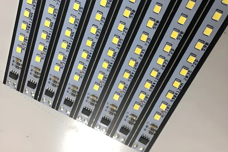
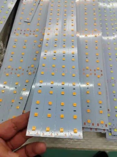
Packaging for Aluminum Substrates (LED Packaging)
LED packaging gives the LED chip a platform to improve optical, electrical, and thermal performance. Good packaging boosts LED efficiency and heat dissipation, which extends life. LED package design is based on five core factors: optical extraction efficiency, thermal resistance, power dissipation, reliability, and cost-effectiveness (Lm/$).
All factors matter. Optical extraction affects cost per lumen. Thermal resistance affects reliability and lifetime. Power dissipation affects the customer application. Good packaging balances these factors and meets customer needs.
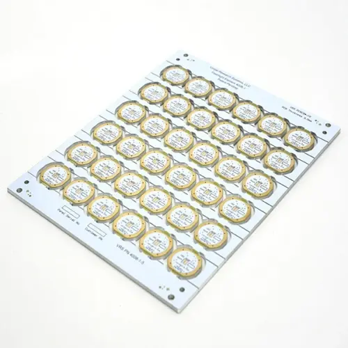
Usually, single-layer or double-layer aluminum substrates are used as heatsinks. One or more chips are die-attached directly on the aluminum (or copper) base. The chip’s p and n electrodes are wire-bonded to a thin copper layer on the substrate surface. Chip count on the board depends on required power; packages can be combined to make 1 W, 2 W, 3 W high-power LEDs. Finally, a high-refractive-index material is molded or dispensed over the LEDs according to optical design.
Aluminum Base Metal Grades
Common aluminum series used for substrates are the 1000, 5000, and 6000 series:
- 1000 series: Examples 1050, 1060, 1070. These are nearly pure aluminum (≥ 99% Al). They are easy to produce and low cost. Widely used in general industry.
- 5000 series: Examples 5052, 5005, 5083, 5A05. These are aluminum-magnesium alloys (Mg ~3–5%). They have low density, high tensile strength, and good elongation. Weight is lower for the same area. Used in aviation (fuel tanks) and general industrial use.
- 6000 series: Example 6061. Containing Mg and Si, this series combines advantages of 4000 and 5000 series. It is heat-treatable, has good corrosion resistance, good machining and coating properties, high strength. Used in aircraft parts, camera parts, couplers, ship fittings, hardware, electronic parts and connectors.
LED Aluminum Substrate vs PCB Aluminum Substrate
LED aluminum substrates are specialized for LED industry and have driven heat-sink applications. They offer high thermal conductivity, low thermal resistance, long life, and voltage resistance. LED aluminum substrates expanded LED uses such as appliance indicator lights, automotive headlights, streetlights, and large outdoor signs.
Thermal conductivity in LED aluminum boards depends largely on the middle dielectric (often a thermally conductive polymer or thermal adhesive). Thermal conductivity, thermal resistance, and voltage withstand are three key quality measures. After lamination, thermal conductivity is measured with instruments. Ceramic and copper materials have higher thermal conductivity, but cost limits most markets to aluminum substrates. Higher thermal conductivity numbers usually mean better performance.
An LED aluminum substrate is essentially a PCB whose substrate material is aluminum alloy instead of FR-4 glass-epoxy.
Aluminum Substrate Pricing
With improvements in production technology and equipment, aluminum substrate prices have become more reasonable. Suppliers usually do not list prices publicly. Contact the vendor (e.g., Yifang Electronics) for a specific quote.
Lead Time for Aluminum Substrates
(A) Order Planning Notes
- Lead time: Prototyping 3–5 days; mass production 5–7 days.
- Quality requirements: Clarify customer details (size, thickness, process, invoice, shipping, special requests).
- Cooperation planning: Confirm whether there will be follow-up volume orders or long-term cooperation.
(B) Ways to Speed Slow Lead Times
- Keep a stock of common aluminum substrates.
- Add day and night shifts to speed production.
- Negotiate adjusted delivery dates with customers.
High Thermal Conductivity Aluminum Substrates and Thermal Conductivity
Thermal conductivity is a key parameter for heat dissipation and one of three main quality metrics (the others are thermal resistance and voltage withstand). Thermal conductivity is measured after lamination. Ceramic and copper have higher conductivity, but cost makes aluminum the mainstream. Thermal conductivity is a core parameter; higher values usually mean better performance.
Aluminum substrates combine good thermal, electrical insulation, and mechanical processing properties. They are widely used in LED and other electronic designs. LED thermal design often uses CFD (computational fluid dynamics) simulation and basic thermal calculations, which are important in substrate production.
Fluid flow resistance (hydraulic resistance) is due to fluid viscosity and solid boundaries. It includes frictional resistance along the flow path and local resistance at abrupt changes (sudden area changes, elbows).
Typical LED heatsink design steps:
- Design heatsink profile under constraints.
- Optimize fin thickness, fin shape, fin spacing, and substrate thickness per heatsink design rules.
- Check calculations to ensure cooling performance meets targets.
Thermal Design for Aluminum Substrates
(A) Why Thermal Design is Necessary
High temperature harms electronics: insulation degrades, components fail, materials age, low-melting solder joints crack, and solder joints fall off.
Temperature effects on components:
- Higher temperature lowers resistor value.
- High temp shortens capacitor life.
- High temp degrades transformer and choke insulation; allowed temperature often < 95 °C.
- Excessive temperature changes solder intermetallic compounds (IMC), making joints brittle and weaker.
- Higher junction temperature (Tj) increases transistor gain, raising collector current and further increasing Tj, which can lead to failure.
(B) Goal of Thermal Design
Keep all components below their maximum rated temperatures in the expected working environment. Max allowed temperatures come from stress analysis and must match product reliability targets and assigned failure rates for each component.
(C) Solutions for Thermal Issues
LED heat is a major pain point. Aluminum substrates, with high thermal conductivity, can pull heat out effectively. Design should keep PCB close to the aluminum base and reduce thermal resistance from potting or encapsulants.
Repair and Maintenance of Aluminum PCBs
Typical repair steps for a PCB technician:
- Fault analysis: Identify and narrow down the board fault.
- Visual inspection: Study inputs/outputs, functions, and control regions.
- Circuit testing: Do initial tests to exclude broad faults and guide repairs.
- Component testing: Often desolder parts and test them with equipment; this may damage outer board appearance, so technicians avoid unnecessary removal.
- Fault repair: Fix traces, replace parts, or modify circuits.
- Functional test: Test the repaired board and run system tests after passing electrical checks.
Waste Handling for Aluminum Substrates
PCBs are made of glass fiber, epoxy, and many metal compounds. Improper disposal of used aluminum boards can release brominated flame retardants and other carcinogens, causing severe pollution and health risks. At the same time, waste boards have high economic value: metal content can be many times that of natural ore. Metal content can be 10–60%, mainly copper, plus gold, silver, nickel, tin, lead, and rare metals. Natural ore metal grades are only about 3–5%.
Studies show 1 ton of computer parts can contain roughly 0.9 kg gold, 270 kg plastic, 128.7 kg copper, 1 kg iron, 58.5 kg lead, 39.6 kg tin, 36 kg nickel, 19.8 kg antimony, plus palladium and platinum. Thus waste PCBs are called “mines to be developed.”
Investigations show most waste PCBs and frame scrap are sent to remote areas for burning or water-washing treatment, causing severe secondary pollution:
- Burning produces strong odors and toxic brominated compounds. This is banned by environmental authorities, but it still occurs in remote areas.
- Water-washing is cheap and simple and widely used. It creates a large amount of residue (non-metal, ~80% of board weight). The residue is hard to dispose of, and many companies dump it as general waste.
Applications and Features of Aluminum Substrates
(A) Application Features
- Excellent thermal conductivity.
- Single-sided copper means components can only be placed on the copper side.
- Cannot open wiring holes like single-sided boards for jumpers.
- Usually used for surface-mount devices; rectifier or power devices dissipate heat via the base, giving low thermal resistance and high reliability.
- Transformers can use flat SMD shapes and dissipate heat through the base, giving lower temperature rise and higher output for the same size.
(B) Hand Soldering Notes
Because aluminum substrates conduct heat well, small-scale hand soldering can cool solder too fast and cause problems. Practical tips:
- Use a household iron with adjustable temperature. Flip it so the flat surface faces up and secure it.
- Set temperature near 150 °C and warm the aluminum board for a short time.
- Then place and solder parts as normal. Use a temperature that makes soldering easier — too high can damage parts or delaminate copper, too low gives poor solder joints. Adjust as needed.