

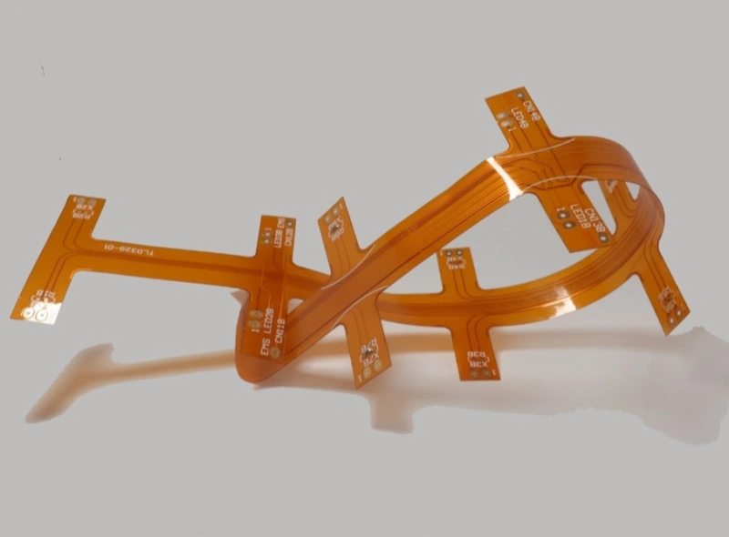
FPC Circuit Design — Common Problems
- Identify the flexible-circuit construction first: copper layers, base film, coverlay or solder mask, stiffeners and the released layer order. The legacy CAD checks below apply only where those features exist; laminated coverlay openings and adhesive clearances need their own fabrication drawing.
- Mark the intended bend regions and state whether flexing occurs only during installation or repeatedly in service. Keep component lands, stiffener transitions and vias out of repeated-bend regions unless the construction has been designed and qualified for them. Agree bend geometry with the flex fabricator instead of applying a universal bend-radius rule.
I. Overlap of Pads
- Check copper-pad clearances and drilled-hole locations separately: overlapping copper pads do not necessarily mean overlapping holes. Remove unintended duplicate drill hits and check closely spaced or overlapping drilled features with the fabricator.
- For a multilayer flex or rigid-flex design, inspect each exported copper layer around pads and vias. An antipad is a copper clearance, while a thermal relief is a copper connection pattern; neither is a separate drilled hole. Confirm that the exported geometry matches the intended net connections.
II. Misuse of Graphic Layers
- Some graphic layers have useless traces. A four-layer board may be drawn with lines like a five-layer board. This causes confusion.
- In legacy Protel workflows, mixing circuit artwork and fabrication annotations on a Board or mechanical layer can produce ambiguous exports. In any CAD tool, inspect the released copper, coverlay or mask, outline and drill files rather than assuming that a layer name defines its manufacturing function.
- Components may be placed on either side when the construction and assembly process support it. Specify the component side, viewing direction and any stiffener-backed assembly areas clearly so mirrored artwork or ambiguous side labels do not reach production.

III. Random Placement of Silkscreen Text
- Text can cover pads or SMD lands. This makes electrical test and component soldering hard.
- If text is too small silk printing is hard. If text is too large letters overlap and they are hard to read.

IV. Hole Size Setting for Single-side Pads
- A single-sided circuit can contain drilled holes, and an SMD land can exist without one. Use the appropriate pad or hole object for the intended feature, then inspect the exported drill file. Do not use a universal zero-hole setting in place of checking the released data.
- For each required hole, specify the finished size and whether it is plated or non-plated, together with its location and any stiffener relationship.
V. Using Filled Areas to Draw Pads
- Copper drawn as a filled area may lack the intended pad, paste, mask or coverlay definitions even if copper DRC passes. Such geometry is not inherently unmanufacturable: inspect the exported openings and the resulting solderable land, and define those features explicitly.
VI. Power or Ground Areas that are Both Thermal Pads and Traces
- A negative-polarity plane layer represents copper clearances differently from a positive copper layer. A thermal relief is a connection geometry, not a reason for the entire layer to invert. Inspect the rendered exported copper and its polarity so the intended connections and clearances are unambiguous.
- When you draw several power or ground isolation groups be careful. Do not leave a gap that causes two power groups to short. Do not block the area that needs connection and split a power zone.
VII. Unclear Definition of Fabrication Stack and Layer Order
- If a single-side board is designed only on the TOP layer and no note is added it is not clear which side is front or back. The made board may be hard to solder after parts are placed.
- For example a four-layer board may be designed as TOP, MID1, MID2, BOTTOM. If the fabricator does not stack layers in the same order problems will occur. So add clear notes about layer order.
VIII. Too Many Fill Areas or Fill Areas Filled with Very Thin Lines
- Photoplot data may be incomplete and data may be lost.
- Legacy photoplot exports may fracture filled areas into many drawn lines. Use an export format supported by the fabricator and inspect the rendered fills, minimum feature sizes and clearances. File size alone does not establish a manufacturing defect.
IX. SMD Pads Too Short
- For dense SMD parts, use lands suited to the component package and soldering process. Plan electrical test access separately with the fabricator or assembler. Where a component land cannot be probed reliably, provide an agreed test point rather than lengthening the solder land only to accommodate a probe.
X. Mesh for Large Copper Areas Has Too Small Pitch
- For hatched copper, confirm the minimum line width and clear opening with the fabricator for the selected copper and imaging process. A 0.3 mm opening is not a universal FPC limit. Check both manufacturability and the effect of the hatch on the circuit’s electrical and bending requirements.
XI. Large Copper Area Too Close to Board Outline
- Keep copper clear of cut edges using the fabricator’s allowance for the selected profiling method, construction and tolerances. A 0.2 mm clearance is not universal. Check coverlay and adhesive clearances as separate features, including areas near bends and stiffeners.
XII. Unclear Board Outline Design
- Some customers draw board outlines on Keep layer, Board layer, Top overlay layer, and these outlines do not match. This makes it hard for the PCB maker to know which outline to use.
XIII. Uneven Graphic Design
- During electroplating uneven patterns cause uneven plating. This affects quality.
XIV. Select Solid or Hatched Copper for the Flex Construction
- Select solid or hatched copper from the electrical requirements, intended bend behavior and agreed flex construction. Hatched copper is not a general remedy for solder-joint voiding or reflow delamination; investigate moisture, coverlay or mask adhesion, materials and the assembly process for the actual defect.
FPC Board Surface Defects and Solutions
The following troubleshooting examples concern FPC flexible boards that use printed solder mask. They are possible causes to verify against inspection and process records, not diagnoses from appearance alone. Laminated polyimide coverlay uses a different application process, so these screen-printing remedies do not apply unchanged. For general exported artwork and drill checks, see the PCB fabrication file checklist.
1. Bubbles Between Tracks or on One Track after Development
Main cause: Bubbles between tracks or on a single track usually happen when track spacing is too narrow and the track height is too high. During screen printing the solder mask cannot reach the base material between the tall tracks. Air or moisture stays between the solder mask and base. During curing and exposure the trapped gas expands and makes bubbles. For a single track the track is too high. When the squeegee touches the track at a larger angle the solder mask cannot reach the track root. Gas stays between the track root and the solder mask. Heat makes bubbles.
Fix: Inspect during screen printing. Make sure solder mask fully covers the base and track sidewalls. Control plating current strictly in electroplating.
2. Solder Mask in Holes and Tiny Pinhole Defects in Pattern
Main cause: When screen printing is not done on time, residual ink builds up on the screen. Under squeegee pressure leftover ink can be pressed into holes. Low screen mesh count also lets ink go into holes. Dirt on the photomask causes areas that should be exposed not to expose. This gives pinholes in the pattern during exposure.
Fix: Do timely screen printing and use higher mesh count screens. Check the photomask cleanly during exposure.
3. Darkening of Copper Tracks under Solder Mask
Main cause: After wiping the board, water was not dried. The board surface got wet before solder mask printing. Or human finger or hand touched the board.
Fix: During screen printing visually check both copper surfaces for oxidation. Make sure the board is dry and clean before printing.
4. Surface Dirt and Uneven Surface
Main cause: Dirt comes from dust and flying fibers in the air. Uneven surface happens when the screen was not cleaned and leftover ink remained on the screen and was pressed to the board.
Fix: Keep a clean room and keep operators clean. Stop non-essential people from walking in the clean room. Clean the room often. During screen printing print on paper in time to remove residual ink from the screen.
5. Misregistration and Fine Cracks
Main cause: Misregistration happens when during screen printing the board is not fixed firmly. Residual ink on the screen is not removed in time and it is pressed onto the board in a pattern, so dots appear near pads. Fine cracks happen when exposure is too weak. Light dose or time is not enough, so small cracks form.
Fix: Use alignment pins to fix the board. Remove residual ink from the screen by printing on paper often. Adjust exposure so the lamp energy and exposure time give a good exposure level. Aim for an exposure index in a suitable range so cracks do not form.
6. Color Difference Between Two Sides and Missing Print (White Spots)
Main cause: The two sides have different squeegee counts during printing. Or old and new inks were mixed. For example one side uses stirred new ink and the other side uses old ink left long.
Missing print or “skip print” happens when electroplating current is too high. The plating builds the line too tall. During screen printing the high line height causes the squeegee not to deposit ink on the track sides. Another cause is the squeegee blade has a nick. The nick area does not deposit ink.
Fix: Keep the squeegee counts consistent for both sides. Do not mix old and new ink. Control plating current. Check squeegee blade for nicks.
Short Summary of Key Checks for FPC Design and Fabrication
- Check pad overlap and hole overlap before making drill data.
- Keep layer use clear and do not misuse Board layer for lines and annotation.
- Place silkscreen text away from pads. Use readable sizes.
- Check each required hole’s finished size and plating status in the exported drill data.
- Check paste, mask or coverlay openings whenever copper fills are used as lands.
- Be clear about thermal reliefs and copper pours. Avoid unintended isolation.
- Document layer stack and build order for the fabricator.
- Avoid too many fill areas or very fine fill lines. Keep data size reasonable.
- Use package-suitable SMD lands and plan reliable probe access or separate test points.
- Agree hatched-copper line widths and openings with the flex fabricator.
- Use agreed copper-to-edge, coverlay and adhesive clearances for the selected process.
- Provide one clear board outline. Do not put multiple different outlines on different layers.
- Balance pattern density to avoid uneven plating.
- Select solid or hatched copper for the electrical, fabrication and bend requirements.

