If you have ever looked at a circuit board and thought, yeah I could never do that. You can.
Not instantly. Not perfectly the first time. But you can absolutely learn how to design a PCB that works, gets manufactured without drama, and does not turn into a week long debugging nightmare.
And honestly, the hardest part is not placing parts or routing traces. It is knowing what to do first, what to double check, and what will bite you later if you ignore it.
So this is a practical walkthrough. The way I would explain it to a friend who has a schematic done and now wants a real board in their hands.
What “designing a circuit board” actually includes
People say “PCB design” like it is one step. It is more like a chain.
- Define requirements and constraints
- Create the schematic (logical circuit)
- Assign footprints (physical packages)
- Create the board outline and mechanical constraints
- Place components with intent
- Route traces and planes
- Run design rule checks and electrical checks
- Generate manufacturing files
- Have it fabricated and assembled
- Test, fix, repeat
You can do steps 2 to 8 inside a PCB CAD tool. The rest is, well. Real life.
Step 1: Start with clear requirements (this saves you later)
Before you open KiCad or Altium or whatever you use, write down a simple checklist.
- What does the board do, in one sentence?
- Input voltage range? Reverse polarity risk?
- Max current on any rail?
- How big can the board be?
- How will it mount? Screws, standoffs, clips?
- What connectors, and where do they need to face?
- Any sensitive signals? High speed, analog, RF, low noise?
- Environment. Heat, vibration, moisture?
- Target cost and quantity
This feels boring but it shapes everything. Like. Whether you need 2 layers or 4 layers. Whether your traces can be chunky and forgiving or need controlled impedance.
Step 2: Capture the schematic (and make it readable)
A PCB starts as a schematic. Even if your circuit is simple, still do it properly.
A few rules that sound annoying but make debugging so much easier:
- Use net labels instead of long wires everywhere
- Group by function: power, MCU, sensors, connectors
- Put decoupling capacitors next to the IC power pins in the schematic too, not just on the PCB later
- Add test points now. You will thank yourself later
- Put part values and part numbers in fields, not in random notes
Also, do not rely on memory for pinouts. Always use the datasheet while wiring symbols. Especially for regulators and USB and anything with multiple grounds or exposed pads.
A quick sanity pass before moving on
Ask yourself:
- Do I have pullups and pulldowns where needed?
- Do I have current limiting resistors for LEDs?
- Did I include programming or debug headers if it is a microcontroller board?
- Is there protection on power input? At least a fuse or polyfuse, maybe a TVS diode if it is an external connector
Step 3: Choose components that exist in real life
This is where a lot of first boards die. In the schematic, any part works. In manufacturing, only parts with good footprints and availability work.
When selecting parts, keep an eye on:
- Package size you can actually solder (0603 is fine, 0402 is annoying, QFN is doable but needs care)
- Supply chain availability. Try not to pick unicorn parts
- Voltage and current ratings with margin
- For connectors, check the mechanical drawing. Do not guess
If you are building something you might reorder later, choose parts from well supported series. Your future self will be less angry.
Step 4: Footprints. The place where mistakes get expensive
Every schematic symbol needs a footprint that matches the exact physical part.
And this is the part where beginners accidentally order ten coasters with copper on them.
Do this carefully:
- Match pin count and pin spacing
- Match the package variant (SOIC is not TSSOP, QFN comes in multiple sizes)
- Check the polarity markers for diodes, electrolytics, IC pin 1
- Verify courtyard and solder mask openings if you made a custom footprint
I like to do this one simple check
Print the PCB 1:1 on paper and place the actual parts on it. Connectors especially.
It sounds low tech. It works.
Before moving to the next step, it’s crucial to perform a thorough PCB inspection to ensure all footprints and placements are accurate.
Step 5: Set up the board outline and layer stack
Now you move to the PCB layout.
Start with:
- Board shape and dimensions
- Mounting holes and keepout areas
- Connector placement constraints (USB at the edge, etc)
- Layer count decision
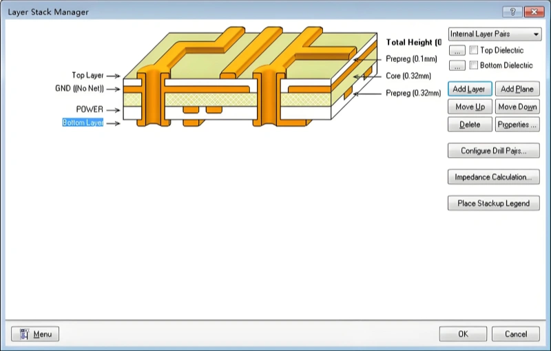
2 layers vs 4 layers
For most hobby and many commercial boards, 2 layers is fine.
But you may want 4 layers if:
- You have high speed signals (USB 2.0, fast edges, DDR, etc)
- You need better ground reference and less noise
- You are routing dense parts like BGAs or lots of fine pitch
- You want power integrity to be easier
A common 4 layer stack is:
Top signal, Ground plane, Power plane, Bottom signal.
Not mandatory. But it is a nice default.
Step 6: Place components like you mean it
Placement is not decoration. It is electrical performance, manufacturability, and sanity.
Here is a practical placement order that works:
- Put connectors and user interface parts first (buttons, LEDs, displays)
- Place power input and power regulation section next
- Place the main controller or main IC
- Place support parts around it (crystal, decoupling, boot resistors)
- Place functional blocks: sensors, drivers, op amps, etc
- Place test points and programming header
Placement tips that prevent noise and weirdness
- Keep decoupling capacitors extremely close to the IC power pins. Not “kinda close”. Like, next to it
- Keep analog sections away from switching regulators
- Keep high current loops tight. Short and wide traces, minimal loop area
- Keep crystals close to MCU and route those traces short, no vias if possible
- Leave space for routing. If everything is packed edge to edge, routing becomes a puzzle you will lose
And also, think about assembly. If the board will be assembled by a factory, they like consistent orientation and enough clearance for pick and place.
Step 7: Define design rules early (clearance, widths, via sizes)
Your PCB tool needs to know manufacturing limits.
Typical safe defaults for many fabs:
- Trace width: 6 mil or 8 mil for signals (wider is easier)
- Clearance: 6 mil or 8 mil
- Via drill: 0.3 mm with 0.6 mm diameter (check your fab)
- Solder mask expansion: fab default is usually fine
But do not guess. Use the manufacturer capabilities. Each fab has a capabilities page. If you are going for cheap prototypes, keep it conservative.
Trace width for current
Signals can be thin. Power traces often should be wider.
If you have 1A or more on a trace, do not run it at 6 mil and hope. Use a trace width calculator or just make it wide and short. Or pour copper.
Step 8: Route the board (and try to keep it calm)
Routing is where people either get obsessed or give up. It is not magic. It is a set of priorities.
Suggested routing order
- Critical signals first
- Clock lines, differential pairs, sensitive analog nodes
- Power routing
- Main rails, high current paths
- Everything else
Ground strategy
If you are on 2 layers, a solid ground plane on one side is gold. Route signals on the other side as much as you can, then stitch ground with vias.
If you must split ground, do it with intention. Most of the time, beginners split ground when they should not. A continuous ground plane is usually better.
A few routing habits that help
- Avoid long skinny traces for power
- Use 45 degree corners or arcs if your tool does it easily. Not because 90 degree corners are evil in low speed, but because it routes cleaner
- Minimize vias on sensitive or fast signals
- Keep return paths in mind. Signals need a return current path under them, typically in the ground plane
Differential pairs (USB, etc)
If you have USB D+ and D-, route as a differential pair with consistent spacing and length matching, and use the correct impedance if your stackup supports it. Your CAD tool can usually calculate widths based on stackup.
If you do not know, that is fine. But do not freestyle and make one trace snake around the board while the other goes straight.
Step 9: Add copper pours, thermal relief, and stitching vias
Copper pours can reduce impedance and help with heat. Common pours:
- Ground pour on top and bottom (connected to GND net)
- Power pours for high current rails if you need
Use thermal relief for through hole pads connected to pours. Otherwise hand soldering becomes miserable and even rework gets harder.
Add stitching vias to connect top and bottom ground pours. Especially around the perimeter, near connectors, and near switching regulators.
Step 10: Silkscreen. Make the board friendly
Silkscreen is not just labels. It is usability.
Include:
- Reference designators (R1, C5, U2) at least for key parts
- Polarity marks for diodes, electrolytics, LEDs
- Pin 1 markers for ICs
- Connector labels. TX, RX, 5V, GND, etc
- Board name, version, date or revision
Leave yourself breadcrumbs. You will come back to this board months later and not remember anything.
Step 11: Run checks before you export anything
Do these in your CAD tool:
- ERC on the schematic (electrical rules check)
- DRC on the PCB (design rules check)
- Unconnected nets check
- Clearance violations
- Annular ring and drill checks
Then do a human check:
- Are all connectors facing the right way?
- Are mounting holes correct?
- Any components on the board edge that will collide with enclosure?
- Did you swap TX and RX. It happens
- Do all polarized parts match the schematic and the silkscreen?
If you can, do a 3D view. Many tools support it now and it catches silly mechanical issues fast.
Step 12: Generate manufacturing files (Gerbers, drills, and notes)
Most PCB manufacturers want:
- Gerber files (or sometimes a single Gerber package zip)
- Drill files (Excellon)
- Board outline
- Readme or fabrication notes (optional but helpful)
- For assembly: BOM and pick and place file (centroid), plus assembly drawings
Export using your fab recommended settings if they provide a preset.
One more thing. Name your layers clearly. And keep versions. “final final v7” is funny until it is not.
Step 13: Prototype like you expect problems (because there will be some)
Order a small batch first. Even if the design is “simple”.
When boards arrive:
- Inspect under good light
- Check for shorts on power rails before plugging anything in
- Bring up power slowly if you can, with a bench supply and current limit
- Validate rails, then clocks, then programming, then peripherals
If something fails, do not panic. Debug systematically. Most early PCB bugs are:
- Wrong footprint or wrong pin mapping
- Missing pullup or pull down
- Power sequencing or regulator stability issues (wrong caps)
- Layout issues around switching regulators
- Grounding or return path issues
- Simple orientation errors
It is normal.
A simple tool stack that works (if you are picking software)
- KiCad: free, very capable, great community
- EasyEDA: convenient if you want quick cloud workflows
- Altium: industry standard, expensive, powerful
- Autodesk Fusion electronics: depends on your workflow
If you are new, KiCad is a strong starting point and it is not a toy anymore.
Common beginner mistakes that are weirdly easy to avoid
Forgetting decoupling capacitors
Most ICs want 0.1uF close to each power pin, plus a bulk capacitor nearby (like 4.7uF or 10uF). Read the datasheet.
Trusting random footprints
Footprints from libraries are helpful, but verify against the datasheet. Always.
Putting the programming header somewhere impossible
If you need to flash firmware, do not hide the header under a display or put it 1mm from the enclosure wall.
No test points
Even just pads for GND, 3V3, 5V, RX, TX. It makes probing possible.
Switching regulator layout “just routed”
Switching regulators have layout guidelines for a reason. Follow the reference layout in the datasheet as closely as you can.
Final thought (and the part where you actually get boards made)
Designing a PCB is a loop. You design, you build, you learn, you revise. The second board is always cleaner than the first.
If you want a manufacturing partner that can take your Gerbers and help you get it across the finish line without guessing, that matters. A lot.
Looking for a reliable PCB manufacturing partner?
Submit your design files to Philifast today and receive a competitive quote with professional support.
FAQs (Frequently Asked Questions)
What are the key steps involved in designing a PCB from schematic to finished board?
Designing a PCB involves a chain of steps: defining requirements and constraints, creating the schematic, assigning footprints, setting board outline and mechanical constraints, placing components thoughtfully, routing traces and planes, running design rule and electrical checks, generating manufacturing files, fabricating and assembling the board, and finally testing and iterating as needed.
Why is it important to start PCB design with clear requirements?
Starting with clear requirements helps shape every aspect of your PCB design. Knowing what the board does, input voltage range, current limits, size constraints, mounting methods, connector needs, sensitive signals, environment conditions, target cost and quantity ensures you make informed decisions such as layer count (2 vs 4 layers), trace widths, impedance control, and component selection that fit your project’s needs.
How can I make my schematic more readable and easier to debug?
To improve schematic readability: use net labels instead of long wires everywhere; group components by function like power sections or sensors; place decoupling capacitors next to IC power pins in the schematic; add test points early on; include part values and numbers in dedicated fields rather than notes; always cross-check pinouts with datasheets especially for complex parts.
What should I consider when choosing components for my PCB?
Choose components that exist in real life with available footprints and supply chain support. Pay attention to package sizes you can solder (0603 is manageable; smaller sizes like 0402 or QFN require care), voltage/current ratings with margin, mechanical drawings especially for connectors, and pick parts from well-supported series if you plan future reorders. Avoid ‘unicorn’ parts that are hard to source or replace.
How do I ensure my footprints match the actual physical parts correctly?
Carefully match pin count and spacing exactly; verify package variants (e.g., SOIC vs TSSOP); check polarity markers on diodes or electrolytics; confirm courtyard dimensions and solder mask openings especially for custom footprints. A practical tip is to print your PCB layout 1:1 on paper and physically place the actual components on it to verify fit before proceeding.
When should I choose a 4-layer PCB over a 2-layer one?
A 4-layer PCB is recommended if you have high-speed signals (like USB 2.0 or DDR), need better ground referencing to reduce noise, must route dense parts such as BGAs or fine-pitch ICs, or want improved power integrity. A common 4-layer stack includes top signal layer, ground plane, power plane, and bottom signal layer which facilitates these needs compared to typical 2-layer boards suitable for many hobbyist projects.