
















What Is a Ceramic PCB?
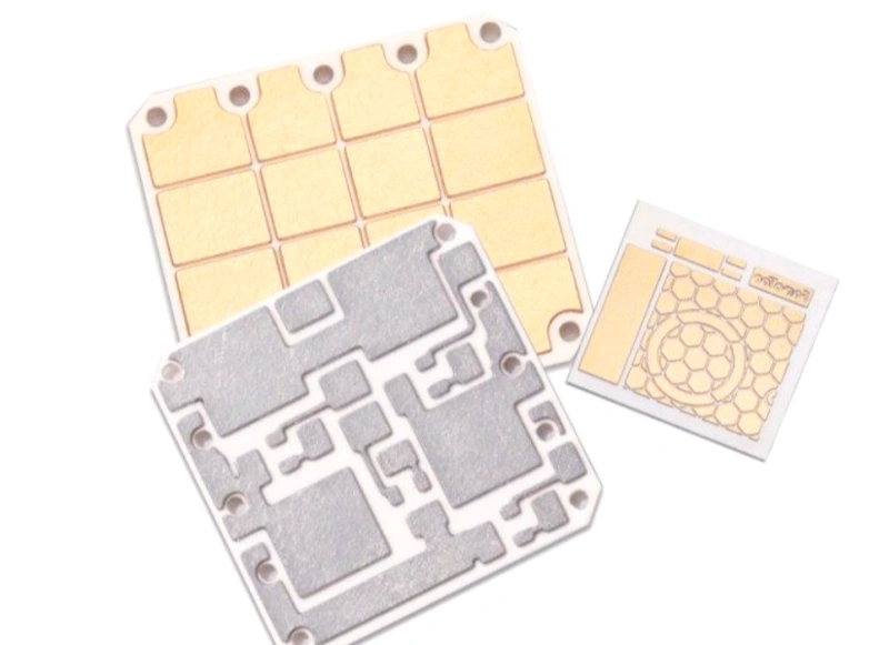
A ceramic PCB uses an inorganic ceramic substrate instead of traditional FR‑4 fiberglass. Common substrate materials are alumina (Al₂O₃), aluminum nitride (AlN), and beryllium oxide (BeO). These boards conduct heat far better than organic laminates. Also, they withstand temperatures up to 350°C for standard alumina and even higher for SiC. Engineers choose ceramic PCBs when they need high thermal conductivity, stable electrical performance at high frequencies, or a coefficient of thermal expansion (CTE) that matches silicon chips. Unlike metal‑core boards, ceramic has no isolation layer between the component and the heat‑spreading material. Components sit directly on the ceramic, which cuts thermal resistance. This direct path keeps junction temperatures low and extends product life.
Types of Ceramic PCBs
There are three main process families. Each suits different performance and cost targets.
High‑Temperature Co‑fired Ceramic (HTCC)
HTCC uses alumina substrate with refractory metal pastes—tungsten or molybdenum. We screen‑print the circuit pattern on green ceramic tape, stack layers, and then fire everything at 1600–1700°C in a reducing gas (hydrogen) atmosphere. The high temperature sinters the ceramic and metal together into a monolithic board. HTCC works well for small, high‑layer‑count substrates. But the extreme firing causes 15–20% shrinkage; we compensate for this scaling during CAM design. The refractory metals have higher resistivity than copper, so HTCC traces show more loss. Use HTCC when you need many layers (up to 10) and can accept wider line widths. Our factory can hold 100 µm line/space after shrinkage correction.
Low‑Temperature Co‑fired Ceramic (LTCC)
LTCC fires at around 900°C. This lower temperature lets us use precious‑metal pastes—gold, silver, or gold‑palladium. The substrate starts as a glass‑ceramic composite tape. We print conductors, punch vias with a laser or mechanical punch, fill them with paste, and laminate the layers. The co‑firing in an oxidizing oven bonds everything. LTCC gives better dimensional control than HTCC (only 0.1–0.2% shrinkage), so we achieve finer lines: 75 µm trace/space typical. Because the fired metal is gold, solder wetting requires special pad coatings. We often add ENIG (electroless nickel immersion gold) as a final finish. LTCC excels for RF and mixed‑signal applications because the dielectric constant is uniform and low‑loss.
Thick Film Ceramic PCB
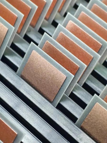
Thick film technology starts with a pre‑fired ceramic substrate (usually 96% alumina). We screen‑print conductive, resistive, and dielectric pastes layer by layer. Each layer fires at 850–1000°C. Conductor pastes are gold or silver‑palladium; dielectric pastes insulate between layers. After firing, we can laser‑trim resistors to ±1% tolerance. Thick film is the lowest‑cost ceramic process for prototyping and moderate volumes. Multilayer thick film copper is a modern variant: we print copper pastes and fire in nitrogen atmosphere. This solves gold‑paste cost and solderability issues. Thick film boards can handle 10–15 µm finished copper thickness, enough for most power circuits up to 10 A.
Ceramic PCB Materials Comparison
Choosing the right ceramic directly affects thermal performance and cost.
| Material | Thermal Conductivity (W/m·K) | CTE (ppm/°C) | Dielectric Constant | Max Operating Temp (°C) | Typical Use Case |
|---|---|---|---|---|---|
| Alumina 96% | 20–24 | 6.5–7.0 | 9.4 | 350 | LED modules, power hybrids |
| Alumina 99.6% | 28–30 | 7.0 | 9.8 | 350 | RF substrates, chip carriers |
| Aluminum Nitride (AlN) | 170–230 | 4.5 | 8.8 | 400 | High‑power GaN amplifiers, EV inverters |
| Beryllium Oxide (BeO) | 260 | 6.4 | 6.7 | 450 | Military radars (toxic—special handling) |
| Silicon Carbide (SiC) | 120‑270 | 4.0 | 40 | 800+ | Extreme high‑temp sensors |
Alumina 96% provides the best price‑performance balance. AlN costs about 3× more but cuts junction temperature by over 20°C in a 50 W design. That extra thermal headroom can double the system’s mean time between failures. Our factory stocks both 96% and 99.6% alumina blanks in 4″×4″ and 6″×8″ panels. AlN blanks are available on request with slightly longer lead times.
Key Advantages of Ceramic PCBs
Exceptional Thermal Conductivity
FR‑4 conducts heat at about 0.25 W/m·K. Even standard alumina (24 W/m·K) moves heat 96 times faster. Aluminum nitride manages 170–230 W/m·K. This means a 1‑ounce copper plane on ceramic acts as an efficient heat spreader. For example, a 2 mm‑wide, 0.3 mm‑thick copper trace at 100 A will rise only 5°C above ambient on an alumina board. The same trace on FR‑4 would overheat and delaminate. Direct component mounting on ceramic eliminates thermal interface material layers, reducing total junction‑to‑ambient resistance.
High‑Temperature Resistance
Our HTCC and thick film alumina boards operate continuously at 350°C. SiC boards go beyond 800°C. Traditional FR‑4 has a glass transition temperature (Tg) of 130–170°C; it softens and fails well below 200°C. This high‑temperature tolerance makes ceramic PCBs indispensable for down‑hole drilling tools, missile guidance, and under‑hood automotive sensors.
Low CTE Matching Silicon and Ceramic Packages
Silicon chips expand at about 2.6 ppm/°C. Leadless ceramic chip carriers (LCCC) have a CTE of 6‑7 ppm/°C. FR‑4 expands at 14–17 ppm/°C. This mismatch causes solder joint fatigue during thermal cycling. A ceramic PCB with 6.5 ppm/°C CTE almost perfectly matches the package. In our reliability tests, ceramic‑to‑LCCC solder joints survive 2,000 thermal shock cycles (−55°C to +125°C) without crack growth, while the same joints on FR‑4 fail after 500 cycles.
Superior Electrical Insulation and High‑Frequency Performance
Dielectric strength exceeds 20 kV/mm on alumina. The dielectric constant stays stable across temperature and frequency, with low loss tangent. This allows high‑impedance‑control traces for RF up to 20 GHz. For mixed‑signal LTCC boards, parasitic capacitance can drop by almost 90% compared to FR‑4 designs. That reduction cuts crosstalk and improves analog‑to‑digital conversion accuracy.
Mechanical Strength and Long‑Term Stability
Despite being brittle, ceramic substrates have high compressive strength (alumina ~2,000 MPa). They resist chemical erosion from fuels, acids, and cleaning solvents. Humidity absorption is near zero, so electrical properties do not drift. Our boards meet IPC‑TM‑650 moisture resistance tests without any degradation.
High‑Density Integration and Miniaturization
We use laser‑drilled microvias down to 0.06 mm diameter. Together with fine‑line LTCC processes (75 µm line/space), you can pack more components in a smaller area. Multilayer co‑firing lets us embed passive components—resistors, capacitors—inside the substrate during sintering. This frees surface area for active chips and connectors. A single LTCC board can replace a whole multi‑board FR‑4 assembly, reducing weight and volume.
Why Use Ceramic PCB Over Other Boards?
Thermal Conductivity: The Real Numbers
FR‑4: 0.25 W/m·K. MCPCB (aluminum back): 1‑2 W/m·K, but still uses a dielectric isolation layer, creating a bottleneck. Alumina ceramic: 24 W/m·K, with no isolation layer. So heat flows instantly from the component pad to the ceramic body. A 10 W LED on an MCPCB might reach junction temperature 120°C; the same LED on alumina stays below 100°C. This cooler operation doubles the lumen maintenance life.
Price Comparison and Total Cost of Ownership
Ceramic boards cost more per unit area. A 2‑layer 96% alumina board (100 × 80 mm) costs about $0.8–1.2/cm² in volume (100‑plus pieces). An equivalent FR‑4 four‑layer board is $0.10/cm². But the system cost tells a different story. Ceramic eliminates the need for thermal pads, heat spreaders, and large heatsinks. For a 50 W power supply, the savings on cooling hardware and assembly labor often exceed $10 per unit. The ceramic version also reduces field returns. Over the product lifetime, ceramic provides a lower total cost of ownership.
Technology Practices: When Ceramic Wins
Use ceramic when:
- Junction temperature must stay below 150°C with high ambient.
- The design has many CTE‑sensitive components (bare die, ceramic packaged ICs).
- You need RF performance above 5 GHz.
- The product faces severe vibration or corrosive environments.
- Miniaturization demands blind/buried vias and embedded passives.
If your constraints are only moderate heat and cost is primary, MCPCB or thick‑copper FR‑4 may suffice. But once you hit a thermal wall, ceramic solves the problem.
How to Manufacture a Ceramic PCB?
We use four main production flows in our factory. I will walk through each simply.
HTCC Process
- Tape casting: We mix alumina powder with organic binder and cast into thin green sheets.
- Blanking and via punching: We cut sheets to panel size and punch or laser drill vias.
- Via filling and printing: Fill vias with tungsten paste. Screen‑print conductor traces on each layer.
- Lamination: Stack layers in a press under heat and pressure.
- Co‑firing: Heat the laminated stack to 1600–1700°C for 32–48 hours in a hydrogen‑nitrogen controlled atmosphere. The binder burns out, and ceramic sinters with metal.
- Post‑processing: Laser trim any embedded resistors. Add surface finishes (ENIG, immersion silver) if needed.
LTCC Process
Same steps but with glass‑ceramic tape, gold paste, and firing at 900°C in air. No hydrogen needed. Via sizes go down to 0.1 mm. We can embed inductors and capacitors inside the stack.
Thick Film Process
- Start with a pre‑fired alumina substrate.
- Screen print conductor layer (gold or silver‑palladium), dry, and fire at 850–1000°C.
- Print dielectric layer to insulate, then fire.
- Repeat for each layer. For thick film copper, print and fire in nitrogen.
- Apply final overglaze or solder mask (if required).
- Laser trim resistors to value.
Typical thick film specifications: line/space 125 µm, via diameter 0.3 mm, up to 4 conductor layers, finished copper thickness 10–15 µm per layer.
Direct Plated Copper (DPC) and Direct Bonded Copper (DCB)
These are simpler methods for single‑ or double‑sided boards. DPC sputter‑deposits a copper seed layer on ceramic, then electroplates to desired thickness. DCB bonds a thick copper foil (0.1‑0.3 mm) directly onto alumina or AlN at high temperature in nitrogen. We use DPC for LED packages and DCB for high‑current IGBT modules. Both deliver excellent thermal performance with copper thicknesses up to 300 µm.
Our factory keeps standard panel sizes: 4″×4″, 5″×5″, 6″×8″, and 8″×10″. Layer counts range from 1 to 6 for thick film, up to 10 for HTCC/LTCC. We achieve 75 µm line/space on LTCC, 100 µm on HTCC. Surface finishes include ENIG, ENEPIG, immersion silver, and pure gold wire‑bondable soft gold.
Ceramic PCB Design Guidelines and DFM Checklist
Designing with ceramic requires special care to avoid cracks and yield loss. I will give you the top rules from our factory’s 15‑year experience.
Via‑to‑Edge Clearance
The most common failure we see is a cracked via near the board edge. Ceramic is brittle. When we depan panelize boards with a diamond saw or laser, micro‑cracks can propagate inward. Keep all via centers at least 2.0 mm from the final board edge. If the design forces a closer via, use tear‑drop pads to reinforce. A teardrop length of 0.5× the pad diameter adds significant crack resistance.
Via Pad and Hole Design
Use tear‑drops on every via and SMD pad. This distributes mechanical stress. Minimum annular ring should be 0.15 mm for Class 3 reliability. Avoid placing vias under BGA corners where stress concentrates during thermal cycling.
Soldering Profile
Ceramic has high thermal mass and conductivity. Preheat becomes critical. Our assembly shop uses a ramp rate of 2.5°C/second, a soak at 150–170°C for 90 seconds, and a peak reflow temperature of 245°C for SAC305 solder. The board must stay above 217°C for only 45–60 seconds to avoid overheating sensitive components. For THT, use a controlled‑heat soldering iron and pre‑heat the board locally. Never apply direct flame.
Component Placement and Handling
Place heavy components (transformers, high‑power resistors) away from edges and corners. Use under‑fill for large BGA packages to manage any CTE difference between the ceramic board and the chip’s organic substrate. During manual handling, use ESD‑safe tweezers with soft tips. Ceramic edges are sharp; wear gloves. Our operators use vacuum chucks to move large panels.
Impedance Control and RF Traces
Ceramic’s dielectric constant (9.4–9.8) differs from FR‑4 (4.5). Always recalculate trace dimensions using a proper field solver, not a generic FR‑4 calculator. For a 50‑Ω microstrip on 0.635 mm thick 96% alumina, the trace width is about 0.6 mm. We provide stack‑up data and controlled‑impedance testing for differential pairs up to 20 GHz.
PTH and Via Fill
We fill vias with conductive paste during co‑firing. In thick film, vias are filled with dielectric or left open. Specify via‑in‑pad design if you need filled and plated‑over vias. We can planarize the surface with a grind process for fine‑pitch BGA.
Applications of Ceramic PCBs
Memory Modules and High‑Speed Digital
High‑speed DDR memory modules benefit from ceramic’s low dielectric loss and thermal stability. Our customers use LTCC boards to route 64‑bit buses with minimized skew. The consistent dielectric constant reduces inter‑symbol interference.
Receiving/Transmission Modules (RF)
Satellite communication transceivers demand low‑loss substrates. Alumina and AlN boards with 0.06 mm laser vias enable compact phased‑array antennas. For a 50 W satellite power amplifier, an AlN board kept peak temperature under 150°C. The design operated reliably in vacuum without convection cooling.
Multilayer Interconnect Boards
Using HTCC/LTCC, we integrate up to 30 embedded passive components inside a 6‑layer board. This shrinks a 4‑board FR‑4 stack into one ceramic module. A customer in the aerospace sector reduced weight by 70% and increased connection density by 5×.
Analog/Digital Mixed‑Signal PCBs
Parasitic capacitance harms ADC performance. With LTCC, we reduced parasitic capacitance between analog and digital sections by about 90% compared to the same circuit on FR‑4. The board’s noise floor dropped by 12 dB.
Aerospace and Avionics
Missile control systems operate at 300°C ambient. Our HTCC boards survive thousands of shock and vibration cycles. No conformal coating needed because ceramic is inert.
Automotive and EV Power Electronics
An electric vehicle charging station uses an AlN DCB board to handle 200 A continuously. Temperature rise stays below 20°C. The board passes IATF 16949 qualification.
High‑Power LED Lighting
A 10 W LED on our thick‑film alumina board shows a junction temperature of 105°C, well below the 120°C limit. The same LED on MCPCB reaches 130°C. This direct bond improves lumen output and lifetime.
Ceramic PCB Procurement: Cost, Lead Time, and MOQ
Realistic numbers help you plan your project budget and schedule.
Ceramic PCB Cost Breakdown
- 2‑layer 96% alumina, thick‑film silver conductor, 100×80 mm, ENIG finish: $8‑12/pc at 100 pieces.
- 2‑layer 96% alumina, thick‑film copper: $10‑15/pc.
- 4‑layer LTCC gold conductor, same size: $25‑40/pc (due to more process steps).
- 1‑layer AlN DPC board for LED: $1‑2 per cm². These prices exclude tooling charges. Tooling (screen tools, photomasks) typically costs $500‑1,000, which we amortize over volume.
Minimum Order Quantity (MOQ)
For standard thick film process, we accept orders as low as 10 pieces. For LTCC and HTCC, MOQ is 50 pieces due to the fixed co‑firing batch size. Prototype runs are available with shorter lead times.
Lead Times
- Thick film 2‑layer prototype: 10‑12 working days (including laser trimming)
- LTCC 4‑layer prototype: 18‑20 working days
- Production orders: 15‑25 days depending on volume
- Expedite service: 5‑7 days possible for thick film using pre‑stocked blank sizes.
We provide rapid quoting within 24 hours after receiving your Gerber files and stack‑up.
Quality and Reliability Standards for Ceramic PCBs
Do not assume all ceramic boards are “high reliable.” Certification matters.
IPC‑6012 Class 3 Certification
We build ceramic PCBs to IPC‑6012 Class 3 for mission‑critical applications. Class 3 requires 100% inspection of via cross‑sections after thermal shock. Our factory performs 6× thermal shock tests from −65°C to +150°C and then micro‑section vias. We allow zero cracks or inner‑layer separation. Annular ring on external pads must be at least 0.050 mm.
Additional Tests We Perform
- Solder float at 288°C for 10 seconds: no delamination, no blister.
- Bond pull strength >5 gf for wire‑bond pads.
- Ionic contamination <1.5 µg/cm² NaCl equivalent.
- Dielectric withstanding voltage 500 V DC for thick film, 1,500 V for co‑fired.
Our factory holds ISO 9001 and IATF 16949 certifications. We comply with RoHS and REACH directives. We use X‑ray inspection on every multilayer LTCC board to verify via alignment.
Challenges and Considerations
Ceramic is not a drop‑in replacement. It requires thoughtful design.
- Brittleness: Ceramic can crack under mechanical shock. Avoid cantilevered mounting. Use brackets or bond the entire board to a metal carrier.
- Limited board size: Maximum single‑piece panel is about 200×200 mm due to warpage during co‑firing. Larger assemblies must use modular designs.
- Lead time for custom materials: Beryllium oxide and AlN blanks sometimes have 4‑6‑week lead times from the substrate manufacturer. Plan early.
- Soldering process: Without preheat, thermal shock can crack the board. Always pre‑heat to within 100°C of solder melting point.
- Cost: For consumer‑volume products, ceramic may be over‑specified. Use it only where the thermal or RF performance advantage pays back.
Frequently Asked Questions
Can you solder to ceramic PCB?
Yes. Solder adheres well to surface finishes like ENIG, silver‑palladium, or thick‑film copper. Use a rosin‑based flux and a controlled pre‑heat to avoid thermal shock. For gold‑paste LTCC, we plate ENIG on pads to ensure solder wets properly.
What is the dielectric constant of ceramic PCB?
Alumina 96% has a dielectric constant of 9.4‑9.8, AlN about 8.8, BeO 6.7. For RF designs, this higher value allows narrower traces for a given impedance compared to FR‑4.
What is the maximum temperature for ceramic PCB?
Alumina and AlN boards can operate continuously at 350°C. SiC boards exceed 800°C. The temperature limit usually comes from the metal paste (gold does not melt, but silver can migrate at high temp under DC bias) and any assembled components.
How do you cut ceramic PCB?
We use laser scribing or diamond saw dicing. Manually, you can score and snap straight lines but expect rough edges. For prototypes, order boards with final outline routing done at the factory.
How thick is a ceramic PCB?
Standard substrate thicknesses are 0.25 mm, 0.38 mm, 0.5 mm, 0.635 mm, 1.0 mm. Thicker substrates up to 2.0 mm are possible for high‑voltage isolation.
What is the price of a ceramic PCB compared to FR‑4?
A ceramic board costs 5–30× more per unit area than FR‑4, but the system‑level cost can be lower when you eliminate thermal management hardware and increase reliability.
Can ceramic PCBs have more than 2 layers?
Yes. HTCC and LTCC easily support 4 to 10 layers. We embed passive components internally, which increases functional density.
Key Takeaways
- Ceramic PCB substrates (alumina, AlN, etc.) conduct heat 100× faster than FR‑4.
- The low CTE matches silicon and ceramic packages, preventing solder fatigue.
- Choose the right manufacturing process: thick film for cost, LTCC for precision/RF, HTCC for extreme high‑temp multilayer.
- Apply DFM rules: keep vias 2 mm from edges, use teardrops, preheat soldering.
- Factor total cost, not just board price; ceramic saves money on cooling and field failures.
- Work with a factory that provides IPC‑6012 Class 3 certification and realistic lead times.
Our team has over 15 years of ceramic PCB manufacturing experience. We support you from material selection to first article inspection. Send your design files or requirements to our engineers for a free design review and cost estimate. We deliver reliable ceramic boards that perform in the toughest environments.