
Smart Home & IoT PCB Manufacturing and Assembly
Connected sensing, control and gateway hardware, built and configured for your product.
FLJ manufactures and assembles customer-designed IoT electronics, from sensor-node and home-control boards to gateway assemblies. We combine PCB fabrication, component sourcing and assembly with specified product integration, firmware programming and functional testing.
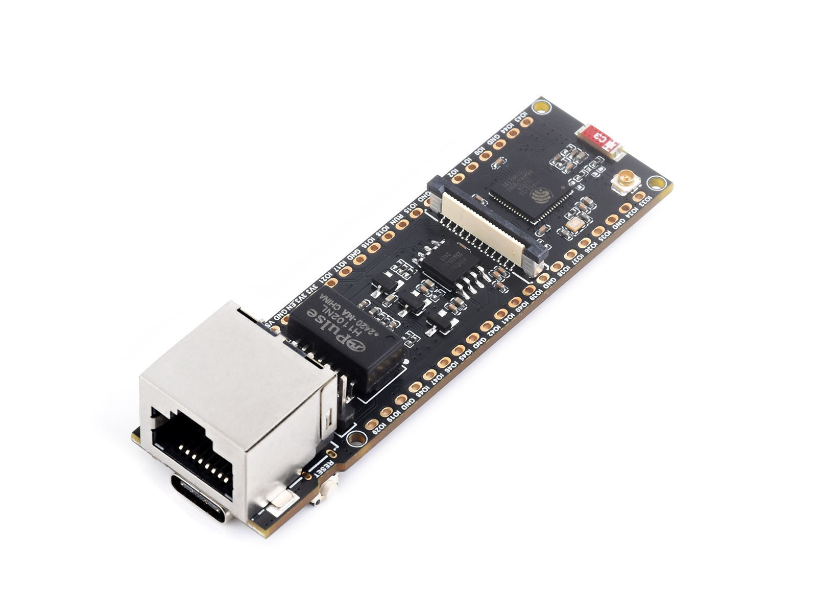
Smart Home and IoT Boards We Manufacture
Connected Sensors and Battery-Powered Nodes
We build sensor-node PCBs and assemblies around the selected sensor, processor, communication interface and power connection. The sensing circuit converts a physical input into a signal or reading that the controller processes and passes to the connected product. Battery-powered nodes can use the specified sleep and wake sequence to schedule processing and radio activity. Presence-sensing boards can instead use a radar front end with a digital-result interface, with the sensor and supply chosen for that product.
Smart Switches and Control Boards
Smart switch, thermostat, and lock-style boards receive a command or sensor input, let the controller select a response, and drive a physical output through the specified switching or driver parts. The board’s terminals, headers, or cable connections carry that output to the product load or actuator. We assemble these customer-designed control boards with the specified controller and interface components, keeping the input path, output device, and product-side connections aligned with the intended unit.
Hubs and Gateway Assemblies
A home hub board joins local sensor or control nodes through the product’s selected radio links or wired interfaces. Its controller and network hardware handle the corresponding connections, while the board provides the specified power, programming and external interfaces. FLJ manufactures and assembles these customer-designed hubs with the selected controller, radio or network parts and connectors matched to the product.
PCB Fabrication and IoT Assembly
Board Construction and Layer Connections
Our rigid PCB fabrication forms the copper circuits, layer connections and mechanical outline for the selected sensor node, controller or hub. For a conventional multilayer build, we form the inner-layer patterns, align and laminate the stack, then drill and metallize the specified connections. The selected outer-layer process forms the surface circuits; solder mask leaves the required lands exposed, and surface finish prepares those areas for soldering. Profiling and mounting features position the board on its product supports.
Where the design includes board-level RF routes, we fabricate the specified signal and reference copper, dielectric spacing, ground connections and connector geometry. These features form the RF circuit structure in the released stack-up. Board density and the actual transmission structure determine the construction, rather than wireless use alone.
Wireless Modules, Sensors and Connectors
Our component sourcing supplies the approved part and package option for each radio, sensor and connector. A radio IC is populated on the main board with its specified support components, which can include power, reset, clock, storage and RF parts. Storage arrangements depend on the IC variant. A preassembled module carries part of the radio circuit on its own board and joins the carrier through its lands or terminals; the carrier still needs its peripheral components and interfaces. The complete part number identifies the required pins, antenna option and hardware variant for assembly.
In SMT assembly, we deposit solder paste through the stencil openings and position the modules, controllers, sensors and passives on their lands with the required orientation. Reflow forms the surface-mount joints; selected through-hole connectors receive their leaded connections. We inspect visible placement and solder features, and use hidden-joint inspection where the selected package and inspection plan call for it. Powered functional checks address the required operating behavior later in the build.

Antenna, Sensor and Housing Integration
Antenna Connections and Required Clearances
A PCB antenna is formed as part of the circuit-board geometry. Its specified position and reserved space are carried through component assembly and installation. Where the product uses an external antenna, FLJ fits the stated antenna hardware and connector and routes its cable as drawn. The released design sets their positions relative to the board, nearby parts and enclosure.
The antenna clearance region and the RF feed’s reference copper have different roles. We keep components and wiring in their specified positions around the antenna, while the fabricated feed and reference conductors retain their required geometry. During board and enclosure integration, we secure the stated connections and cable route and preserve access for mating and closure. Actual clearances follow the selected antenna and product drawing.


Sensor Access and Housing Assembly
We locate the sensor and its connections in the position and orientation defined for the product. For presence radar, the installed direction, configured sensing region and response delay affect which target conditions produce an occupied or clear output and when it changes. The assembly preserves those relationships. Any required opening, exposed surface or contact path follows the selected sensor’s function and installation drawing.
For orders that include enclosure work, FLJ fits board supports, internal connections and cables, then checks connector access and cover fit before closure. Supports locate the board; cable routing and strain relief reduce handling forces at the terminations. Where selective conformal coating is specified, we apply the defined coverage while leaving the required mating contacts, test points and sensor-access areas clear.
Firmware Programming and Product Configuration
FLJ matches the released firmware and product settings to the specified board revision, controller and radio variant. Our IC programming service uses the supported method for the device and build: a matching socket before assembly, or accessible connections on the populated board. Supply, reset and protection conditions follow that target’s programming requirements.
We identify the selected image and verify the programmed regions using the comparison or checksum method supported by the target and tool. The file identifier tracks the release; programmed-data verification checks the covered memory and settings. The assembly then receives the powered operating checks specified for its product.
For products with retained operating parameters, we apply the defined write-and-save sequence and check the stored settings by the specified method. Where unit-specific data is included, the agreed fields, supplied values and storage locations form part of that programming scope. Shared settings and assigned unit identifiers are kept distinct and carried into the applicable delivery identification.
Functional Testing for Connected Devices
Power States and Sensor Response
FLJ runs a product-defined functional test sequence with the released firmware, configured settings and specified supply. A power-state check identifies the startup, sleep or wake state, or the defined event being triggered, along with its observation window, measurement point and acceptance limit. Module-supply and whole-board readings cover different loads. The measurement path must preserve the required supply voltage as current changes. If transmission is included in the check, the procedure triggers an identified radio event and observes its specified response.
For a presence-sensing assembly, the test fixes the installation condition, sensing region, firmware settings and response delay before comparing the observed state with the product requirement. The selected input and observation point define which part of the sensing and control path the check covers.

| Input method | Applied condition | What the observation covers |
|---|---|---|
| Physical target | Place the prescribed target in, or clear it from, the configured sensing region using the defined installation and timing. | The sensor front end and processing through to the selected reported or controller response. |
| Electrical input | Inject the defined signal at the identified controller interface with the required firmware and settings. | The response from that interface onward. This starts downstream of the physical sensing front end. |
Illustrative test scope. Each path uses its product-defined expected response and timing criteria.
Communication and Control Outputs
A communication check names the interface and known peer, applies a defined request or event, and checks the expected returned fields within the product’s response window. The transaction ties the observed data to a particular path and condition. When a command controls a load, the test also connects the required load and observes the actual electrical output at its designated board point; a returned status by itself does not show that the load received the required output.
FLJ prepares the connections and, where required, product-specific fixtures and test programs for the supply, stimulus, communication and load paths. Each sequence associates an applied condition with its observation point and acceptance criterion, keeping the result tied to the assembled board and its configured firmware.
Send the PCB files, BOM and assembly requirements, together with the applicable firmware, antenna or housing details and functional-test requirements for your product.