
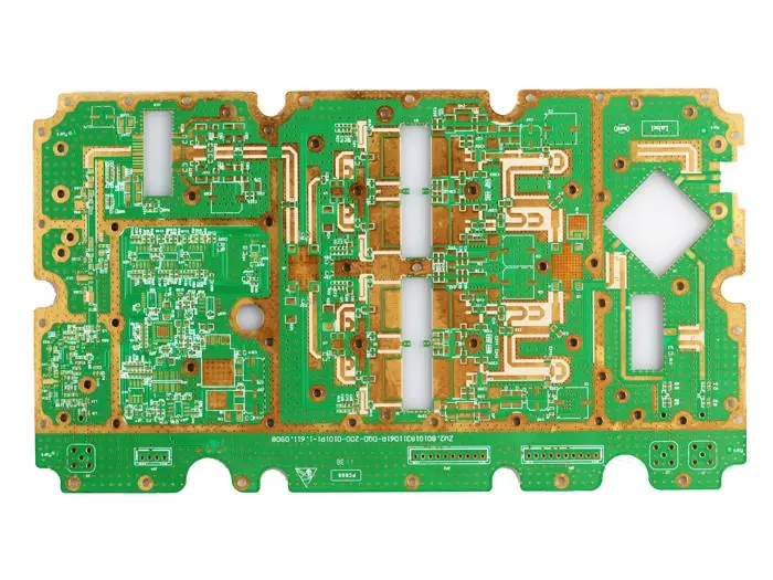
8-Layer PCB Manufacturing
Custom eight-layer boards for dense interfaces, multiple supply rails and controlled-impedance routing. FLJ fabricates prototypes and production batches with the laminate, copper build, plated connections and surface finish specified for your product.
Bring a completed layout or work with our manufacturing team on the stackup while the design develops. Bare-board fabrication and PCB assembly are available through one manufacturing partner.
- Layer structure
- 8 copper layers · custom allocation
- Fabrication options
- Laminate · copper · finish · vias
- Order scope
- Prototype, production & assembly
Eight-Layer Boards for Interface-Dense Electronics
An eight-layer PCB gives a complex circuit more ways to separate routing, reference planes and power distribution within its mechanical outline. The value comes from assigning those layers to the circuit’s actual needs: escape channels around a dense device, continuous references for fast interfaces, or space for several supply domains.
Networking and communication boards
Switch, gateway and communication boards bring connector fields, transceivers and their supply circuits into a shared outline. Internal routing layers carry connections across the board while nearby reference copper supports the intended transmission-line geometry. Material loss and via transitions become important as channel length and signal bandwidth increase.
FPGA, SoC and memory boards
Processor-memory boards and FPGA carrier designs create a routing task beneath the package as well as across the board. Additional internal layers provide destinations for escape routes, and allocated planes serve the power and reference networks. The pin map, pad pitch and via geometry determine whether those layers are accessible.
Embedded and industrial electronics
Processors, analog inputs, communication ports and power circuits can occupy the same board. An eight-layer build creates room to organize those functions and their connections without forcing every route onto the outer faces. The electrical arrangement and mechanical fit remain part of the same fabrication specification.
Allocate Routing, References and Power
Eight copper layers can support different balances of signal routing and planes. The examples below retain four signal layers while changing the ground and power allocation. They illustrate electrical roles; neither is a universal manufacturing stackup.
Four signals, three grounds and one power plane
- L1SignalRouting
- L2GroundReference
- L3SignalRouting
- L4PowerSupply
- L5GroundReference
- L6SignalRouting
- L7GroundReference
- L8SignalRouting
L1 and L3 have L2 ground beside them. L6 lies between the ground layers on L5 and L7, and L8 is next to L7 ground. L4 power and L5 ground form an adjacent plane pair. This arrangement spends more of the eight-layer resource on ground references while retaining a dedicated power layer.
Four signals, two grounds and two power planes
- L1SignalRouting
- L2GroundReference
- L3SignalRouting
- L4PowerSupply
- L5PowerSupply
- L6SignalRouting
- L7GroundReference
- L8SignalRouting
Two internal power layers provide additional space for supply distribution. Their copper regions serve the intended supply networks, with plane partitions coordinated with nearby signal routes. The outer signals still sit beside ground, as do L3 and L6 on one side. Those inner signals also face power copper on the other side, so the dielectric spacing, supply regions and nearby conductors all contribute to their electrical environment. The two central power layers also couple to each other; their spacing and rail arrangement are part of this choice.
Turn the allocation into a fabricated structure
The copper roles are only one part of the build. Eight copper layers have seven dielectric regions between them. In one conventional foil construction, three double-sided cores form the six inner copper layers, with prepreg bonding regions between the cores and beneath the outer foils.
A bonding region may contain several prepreg plies. Its pressed thickness depends on the material construction, resin and copper pattern. Electrical roles do not establish material thickness or mechanical balance by themselves. FLJ develops the fabrication stackup around the selected material, finished copper and required geometry.
Material and Fabrication Options
Configure the board as a complete product: laminate system, finished thickness, inner and outer copper, exposed pad finish and interconnections. These choices influence both the physical build and the electrical channel.
Bring the selected material, copper and finish together in one eight-layer fabrication quotation.
Discuss your board configuration →Interconnects for Dense Packages and Fast Interfaces
Layer count creates routing resources. Interconnect geometry determines how the package and signals reach them. Through vias, selected blind or buried connections, filled via-in-pad structures and backdrilling address different constraints within an eight-layer design.
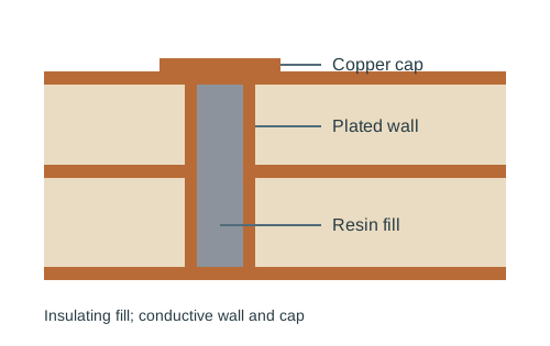
Escape routing and a usable solder pad
When the pad spacing leaves little room for an external fanout, a via in the pad moves the connection into the pad area. An untreated opening can draw solder away during assembly. Filling, planarization and copper capping provide a pad surface suitable for the intended assembly process.
In a resin-filled plated via, the hole-wall copper carries the electrical connection. The resin fills the interior, and the copper cap forms the surface above it. Copper-filled microvias use a different construction and process. The required span, hole geometry and subsequent connections determine which approach fits the design.
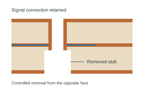
Control the transition as well as the trace
A through via can extend beyond the layer where the signal leaves its barrel. That unused portion is a stub. For a suitable high-speed design, backdrilling removes part of the unused barrel while preserving the connection that the circuit needs. Removal depth and clearance must leave the intended connection intact. The hole drawing distinguishes the connected span from the section to remove, rather than applying the same depth to every via.
Backdrilling and filling solve different problems. One controls the remaining barrel; the other establishes a filled structure or pad surface. Signal transitions also need a suitable return path when their reference changes. A filled hole or a short stub does not by itself establish that return connection.
An eight-layer board can use conventional mechanically drilled through vias. HDI is an interconnect choice for the actual density and escape requirement, rather than a consequence of the number eight.
Local construction illustrations, not complete eight-layer cross-sections. Not to scale; no drilling dimensions or process limits are specified.
Building and Verifying the Eight-Layer Board
FLJ manufactures the internal circuits before laminating them into the completed stack. Inner-layer optical inspection checks the copper while it is accessible. Registration and lay-up align the patterned cores, bonding materials and outer copper; drilling and metallization then create the specified connections through the construction.
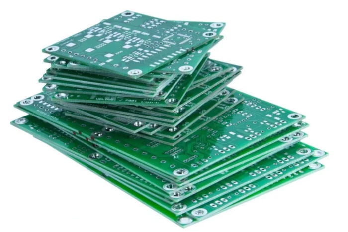
Inspection follows the manufactured feature
Before lamination, the internal copper is exposed for optical checks. This is the opportunity to find circuit-pattern defects before the layers are enclosed. Layer registration then connects the stackup drawing to the actual position of pads, holes and copper through the board.
After hole processing, inspection focuses on the manufactured connection: the plated wall, filled region and copper cap where specified. Cross-sections reveal selected internal dimensions and interfaces in the prepared sample. These observations complement the dimensional checks of the finished outline and hole locations.
Electrical continuity and isolation testing examines the board’s connection network. For controlled impedance, the defined coupon and test address the representative transmission-line geometry. Neither result alone measures the complete system’s channel loss, device operation or EMC.
Prototype and production builds
The fabrication definition links the initial build to later batches: material grade, layer order, pressed dielectric construction, finished copper, hole structures and finish. Keeping that definition clear makes a repeat order more meaningful than repeating only the words “eight-layer PCB.”
Prototype findings can refine the production construction. The accepted material and geometry then provide a defined basis for later batches; a proposed material substitution is assessed against both the fabrication process and the electrical model before it becomes part of that build.
Compare the Complete Six- and Eight-Layer Build
Compare what the extra layers make possible in the same circuit. They may provide another reference plane, more power distribution space or additional routing capacity. They are valuable when that allocation resolves the layout’s real constraint. A six-layer design that needs long detours or a more complex interconnect to preserve references can justify a different comparison from a six-layer board that already routes cleanly. Hold the board envelope and electrical objectives constant when evaluating the alternatives.
| Design situation | What to compare |
|---|---|
| Routing fits in six layers with suitable references | The existing six-layer construction against the cost and benefit of adding layers. |
| More plane resources are needed around several interfaces | An eight-layer allocation that preserves usable routing while providing the required references and supply regions. |
| The package cannot escape within the available geometry | The pad map, via approach, trace space and accessible signal layers together. |
| Price differs between proposed builds | Material, thickness, copper, panel use, hole processes, finish, inspection and order quantity. |
The additional layers use material and manufacturing resources, but a fixed six-to-eight-layer price multiplier cannot describe every design. Special interconnects, filling, backdrilling or added process stages can matter more than layer count alone. Batch preparation costs and the number of usable boards on the working panel also affect unit cost.