
Telecommunications PCB Manufacturing & Assembly
Custom circuit boards and assemblies for network interfaces, gateways and RF communication hardware.
FLJ combines PCB fabrication, component sourcing and assembly for prototype and production builds. Choose bare boards, populated PCBAs or an assembly completed with the specified equipment connections.
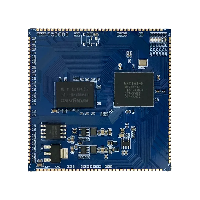
Network Boards for Routers, Switches and Gateways
FLJ builds network and gateway boards that connect processor and memory packages to data ports, peripheral interfaces and power inputs. Fabrication and component assembly carry those connections into the supplied board.

Dense Processing and Board Interconnects
Package escape starts at the device pads. In high-speed PCB manufacturing, patterned copper forms the routes, lamination sets the dielectric separation, and plated copper connections join the specified layers. For dense pad fields, a selected HDI construction uses shallow microvias to reach nearby routing layers while preserving space deeper in the board.
Where the package uses via-in-pad, the specified filling, planarizing and copper-capping process creates a continuous soldering land. FLJ sources the specified processor, memory and interface components, prints solder paste, places the parts and completes the required soldering. Fine-pitch and BGA devices are assembled on their prepared lands with the orientation and thermal process suited to the selected components and board.
Network and Power Connections
Network jacks, peripheral sockets and power connectors turn the populated circuit into accessible equipment hardware. Surface-mount contacts are soldered to their lands; connectors with leaded terminations receive through-hole assembly. Connector seating and orientation preserve the intended mating position, while the soldered pads and plated holes carry data and power into the board.
RF and Wireless Communication Boards
FLJ fabricates and assembles RF front ends, transceiver circuits and mixed RF/control boards. In designs with an external antenna connector, the signal path continues from the radio device through the PCB and into the connector, together with its reference connections.
RF Signal Paths and Board Construction
An RF trace works with its reference copper and the dielectric between them. RF board fabrication forms the line, adjacent ground and clearances through imaging and etching. The selected lay-up and lamination establish the material stack and dielectric spacing. Where the route changes layers, plated signal vias and ground connections provide the corresponding signal and return paths.
At a coaxial board connector, the center contact meets a signal pad or taper, while the outer contacts join reference copper through ground pads and vias. Footprint clearances, board thickness and contact positions define this local transition. A compatible hybrid construction can combine RF material layers with control and power routing, using the material and bonding arrangement selected for the complete stackup.

RF Components and Connector Assembly
During RF component and connector assembly, FLJ places the specified devices and completes their surface-mount or through-hole connections. Connector seating and solder wetting establish contact at the signal pad and ground contacts. The solder joint’s shape becomes part of the RF transition as well as its mechanical attachment, so the footprint and assembly drawing guide the finished connection.
Specified shield parts are fitted to the drawing as supplied mechanical and grounding components. Inspection then examines the soldered connections and component positions against the assembly requirements.

Integration into Communication Equipment
For an installed assembly, box build integration brings the PCBA, supports and equipment connections together. FLJ mounts the board on its specified supports and aligns the ports with the panel openings. Cables are routed and secured with the required keying, clearances and strain relief, keeping installation loads away from their terminations. Specified thermal contacts connect the designated board or component surface to the equipment’s heat-transfer interface.
Where protection is required, conformal coating covers the designated circuit areas while mating surfaces and test contacts remain accessible. These operations follow the selected delivery scope, completing the physical board-to-equipment connections before the final interface checks.

Telecom PCB Inspection and Functional Testing
FLJ provides bare-board electrical checks, assembly inspection and product-specific functional testing. Each examines the relevant circuit connections, fitted components or powered response of the communication hardware.
Inspection of Boards and Soldered Connections
Before assembly, bare-board electrical testing checks continuity within the intended nets and isolation between them. On a populated board, AOI inspection compares visible connector placement, orientation and solder features with the assembly reference. Selected BGA connections can be examined by X-ray beneath the package; the observed joint pattern is interpreted with the array position and overlapping structures in view.
Powered Interfaces and Communication Response
IC programming loads the released firmware and settings for the hardware. Functional testing then applies the product’s defined operating conditions and checks its response. For a gateway interface, this can mean sending a specified request and evaluating the returned message or state within the required response window. An integrated unit is checked through its selected external ports after the specified cables and enclosure are assembled.
Example of a defined gateway-interface check. The product test plan sets the connection, firmware, stimulus and acceptance criteria.
Send the PCB files, BOM, assembly drawings and required delivery level to discuss fabrication, assembly and the checks for your project.