
PCB Surface Finishes
Match the exposed copper finish to your assembly process and the way the board will be used. FLJ helps review ENIG, HASL, OSP, immersion finishes and plated gold options with your design.
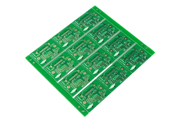
What is a PCB surface finish?
A PCB surface finish protects exposed copper and provides a surface for soldering or electrical contact. It is applied to areas such as component pads and contacts; it is different from the solder mask covering the rest of the board.
The right finish depends on pad geometry, assembly cycles, storage and contact use. A fine-pitch component pad and a connector finger do not have the same job. We consider those differences when reviewing a finish callout, so the manufacturing choice supports the next production stage.
If your files already specify a finish, send that information. If it has not been chosen, tell us how the board will be assembled and whether it has exposed contacts. We can discuss the practical options without asking you to settle every process detail first.
Compare common finish options
These finish families are included in FLJ’s published capability information. Selection is reviewed against the material and the intended assembly or contact application.
| Finish | Where it is often considered | Selection point |
|---|---|---|
| ENIG | Flat soldering surfaces and fine-pitch layouts | Nickel/gold process, assembly compatibility and cost |
| Lead-free HASL | General soldered PCB assemblies | Pad topography and small-component geometry |
| OSP | Copper soldering surfaces with a thin organic coating | Handling, storage and the planned assembly sequence |
| Immersion silver | Flat soldering surfaces and selected RF designs | Packaging, exposure and handling conditions |
| Immersion tin | Flat soldering surfaces and selected assembly processes | Storage and the full assembly thermal history |
| Electroplated hard gold | Repeated mating contacts and connector fingers | Contact area, wear requirement and plating callout |
| ENEPIG or soft-gold routes | Selected bonding and specialty applications | Package or bonding process and agreed finish specification |
Soldering pads and connector contacts need different finishes
Flatness can matter when solder paste deposits and component standoffs are small. ENIG and immersion finishes are commonly considered for flat-pad constructions, while HASL should be reviewed against the actual component geometry. There is no single finish that is automatically best for every assembly.
Connector fingers may need a wear-resistant plated surface because they are used for repeated electrical contact. That is a different purpose from a solder pad. For these boards, send the connector arrangement and expected contact use so we can discuss selective plating and any edge or chamfer details.
Wire bonding and other specialty processes need their own finish review. Share the intended bonding method or package guidance rather than choosing by the finish name alone.
Combined finishes and material compatibility
FLJ’s published options include combined treatments such as ENIG with gold fingers and OSP with electroplated gold. These allow soldering regions and contact regions to receive different treatments where the construction supports them.
The finish route also depends on the substrate. A ceramic, flexible or high-frequency board may have a different set of suitable processes from a conventional rigid FR4 board. We review the material, exposed features and assembly sequence before agreeing the treatment.
Finish thickness is specified by the selected process, application and acceptance agreement. We confirm the applicable callout for your order instead of presenting one gold, silver or tin thickness as a universal capability for every board type.
Storage, handling and documentation
A surface finish works with the packaging and handling plan. Tell us if bare boards will be stored before assembly, shipped to another assembler or run through several thermal cycles. This helps us review the finish and packaging together.
During assembly, clean handling and suitable storage protect the exposed pads. For repeat orders, the finish callout should stay aligned with the approved drawing so purchasing and receiving inspection refer to the same treatment.
If you need a finish measurement report or other process documentation, we can discuss its scope when preparing the quotation. Material compliance documents and quality-system certificates remain separate from the finish specification.
Finish specification and measurement
Send the finish already shown on your drawing, or tell us how the board will be assembled and used. We can review the appropriate process and documentation.
| Finish | Specification to review | How we help |
|---|---|---|
| ENIG | Nickel and gold thickness; pad planarity | Review drawing callouts and the selected supplier process |
| ENEPIG | Nickel, palladium and gold layers | Connect the finish with bonding or soldering requirements |
| Plated gold contacts | Gold thickness, underlying nickel, contact region | Match insertion/wear needs and the specified connector area |
| Immersion tin / silver | Deposit requirement, handling and assembly sequence | Review the current finish specification and protective packing |
| OSP / HASL | Coating or solder coverage and surface geometry | Match storage, soldering sequence and component pad geometry |
| Verification | Agreed thickness record or measurement report | Discuss the method and sample locations needed for your supplier review |
Finish thickness and storage conditions are specific to the selected process. They are agreed with your project rather than copied from a generic finish table.
Send your drawing for a finish review
A Gerber package, drawing or existing board specification gives us a starting point. Add any known assembly process, connector contact requirement or storage concern. If those details are still developing, our team can follow up and help identify the useful questions.
We can then compare the available finish routes with the layout, substrate and production plan, and include the agreed treatment in the quotation. Any proposed change from a named finish is discussed with you before production.
Frequently asked questions
Is ENIG always better than HASL?
No. ENIG offers a flat pad surface, while HASL can suit many conventional soldered boards. The component geometry, assembly process and cost should guide the choice.
Can gold fingers and solder pads use different finishes?
Yes, combined finish routes are part of FLJ’s published options. Send the contact regions and pad layout so we can review the appropriate process.
Is the surface finish the same as solder mask?
No. Solder mask covers and protects selected board areas. The finish treats copper left exposed for soldering or electrical contact.
What if my designer has not specified a finish?
Send the files and explain the application. We can review the pad geometry and assembly needs with you, then agree a practical finish.
Explore related capabilities
Let’s review your next build
Send your available board files, drawings or project questions. Our team will review the information and follow up with you about the next step.