
PCB Files &
Gerber Guide
Understand your PCB files, explore the common export options and get help preparing your board for manufacture.
Already have a design package? Send it to FLJ PCB. Our engineers will review what is available and contact you if an additional file or detail would help.

What is a PCB file?
A PCB file is the electronic description of a circuit board. In a design tool, it brings together the outline, footprints, copper routing, holes and layer information. A schematic is the related circuit diagram: it explains the electrical connections rather than the physical board layout.
Different design tools save projects in different ways. You may see an Altium .PcbDoc, a KiCad .kicad_pcb, or a .brd file from another CAD system. The software name is useful because an extension alone does not always identify the tool or its version.
You can send your existing design files or exported manufacturing package when starting an enquiry. We’ll review the package and discuss the most useful output for your board.
What are Gerber files?
Gerber is a widely used way to exchange PCB manufacturing data. A conventional package describes the copper and other board layers as separate outputs. Opening those outputs together gives a view of the board that can be used for manufacturing review.
Copper layers describe the conductive features. Solder mask shows where the protective coating opens to expose pads. Silkscreen, also called legend, contains markings such as reference designators. The profile describes the board’s perimeter and internal cutouts.
Gerber X2 adds attributes that help identify layer functions and features. Names and extensions still vary between CAD tools, so a recognizable layer list is helpful. Our team can review the files with you if their names are unfamiliar.
What do the different outputs show?
| Output | What it helps explain | A useful example |
|---|---|---|
| Copper layers | The conductive pattern on each board layer | Top, inner and bottom copper |
| Solder mask and legend | Exposed surfaces and printed markings | Top mask, bottom mask, component labels |
| Board profile | The finished shape and cutouts | A board outline or Edge.Cuts output |
| Drill data | Hole locations and sizes | Plated holes, mounting holes and slots |
| Drawing or construction notes | The physical construction and special details | Thickness, material, finish and dimensions |
This is a guide to the information you may encounter, not a condition for making an enquiry. Send the outputs you already have and we can help identify their role.
How drill files describe the holes
Drill data connects each hole location with a tool size. Excellon-style NC drill files are common and may use .drl, .txt or another extension. A drill map is a visual companion that makes the hole types easier to discuss.
Plated through holes provide a conductive connection through the board. Non-plated holes are often used for mounting or mechanical features. Slots describe elongated openings; a drawing can help explain their finished dimensions.
Many CAD tools offer separate plated and non-plated exports, along with a drill map. If your package uses another arrangement, our engineers can look at it and discuss how the hole information is represented.

How to export and view a manufacturing package
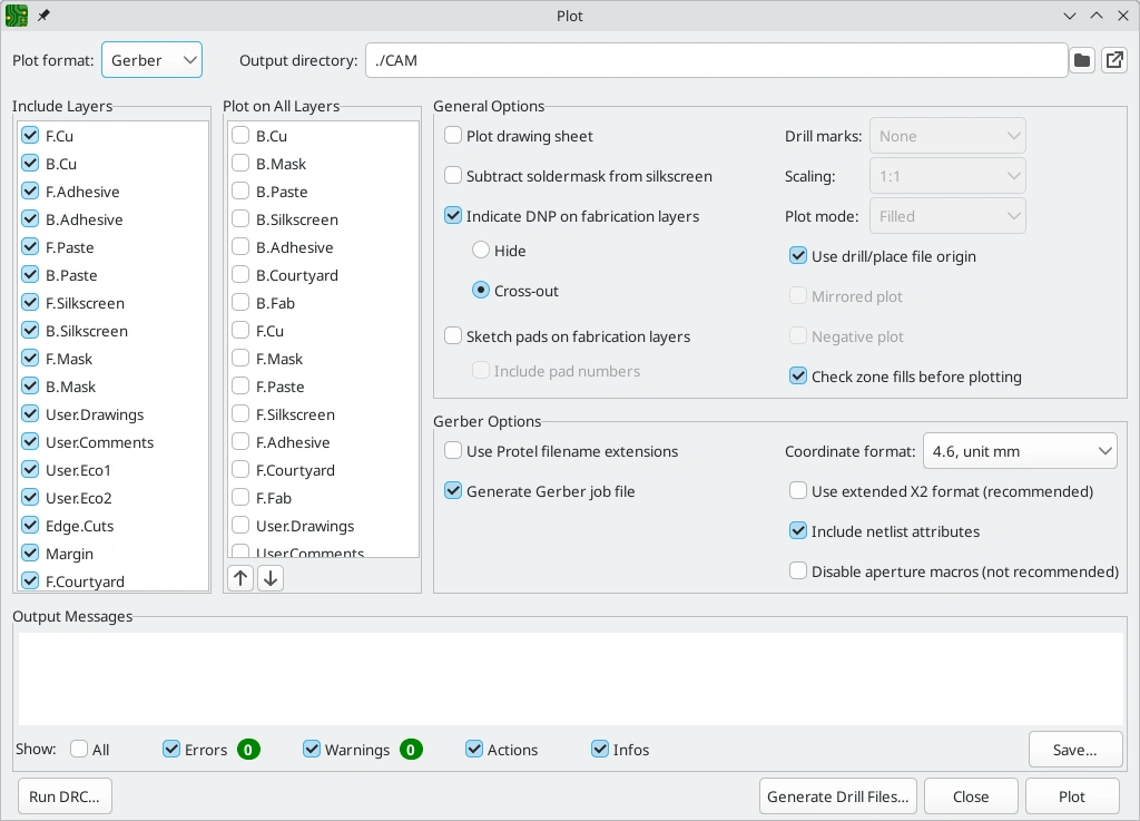
Start in the PCB editor for your design tool. Look for plotting, fabrication outputs, CAM or an output-job menu. Select the board layers and export the Gerber data, then generate the drill outputs. The exact menu names depend on the software and version.
Open the exported layers in a Gerber viewer. You can turn individual layers on and off to look at the outline, pads, mask and holes. This is a useful way to see the manufacturing outputs independently of the design editor.
Altium output jobs, KiCad plotting and other CAD export tools offer different workflows. If you would like help, tell us which tool you use and share the available package. We can discuss the relevant export or conversion route.
Adding a little context about the board
A few construction details help turn the files into a quotation. Board thickness, layer count, material and surface finish are useful starting points. If these choices are still open, explain the application and we can discuss options.
For a multilayer board, a stackup describes the sequence of copper and insulating layers. For a controlled-impedance design, the relevant traces, target impedance and reference layers help the engineering conversation. A drawing or existing stackup is useful when available.
Quantity can mean individual boards or complete panels. Tell us how you would like the boards supplied, and we can discuss panelization if it would help assembly or handling.
Already have another file format?
Gerber is a common starting point, but your designer may have prepared native CAD data, ODB++, IPC-2581 or another output. Send the package you have and tell us the design tool if you know it. Our engineers will review the data and help identify a practical route to manufacturing.
A PDF or board photograph can also help explain a question or an existing product. It provides visual context; the team can then discuss any additional design or manufacturing data needed for the project.
For a bare-board enquiry, assembly placement data usually comes later. If you also want the boards assembled, our PCB assembly file guide explains how the parts list and placement information fit in.
Your questions, answered
Can I send a native PCB design instead of Gerber?
Send the files you have and identify the CAD tool where possible. We’ll review the package and discuss any helpful manufacturing export or conversion.
I have a ZIP from my designer. What should I do with it?
You can send the ZIP for review. If you know the board revision and quantity, include them in the message. Our team can help identify the files inside.
Do I need to rename all the Gerber files?
Usually your CAD export names provide a starting point. A layer list is helpful if the names are ambiguous; we can discuss those with you during review.
Can you help before I have chosen material or finish?
Yes. Explain the application and any important electrical, thermal or assembly needs. We can discuss suitable construction options for the enquiry.
Share your PCB files
Send the board data you have, or tell us what you would like help exporting. Quantity and a short project description give us a useful starting point.
Email [email protected] with your files or question. Our team will review the information and follow up with you about the next step.
Explore the technical details: Ucamco Gerber documentation · KiCad PCB Editor documentation. Software examples illustrate the tools; your design may use a different workflow.