
High-Speed Digital
PCB Manufacturing
The signal path, built into the board.
FLJ manufactures high-speed digital PCBs with low-loss material options, controlled-impedance circuitry and the interconnections needed by the design. From the etched conductor to the back-drilled via, our fabrication work turns the stackup and layout into a physical signal path.
Prototypes & production • Bare boards & PCB assembly
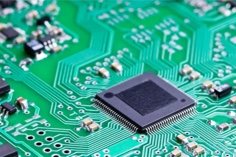
High-Speed Boards for Digital Interfaces
A network link, a processor-to-memory connection and a connector-to-connector channel place different demands on a PCB. FLJ builds the board around those connections, combining material, copper layers and via structures in the required outline.
Networking & interconnect boards
Switch, communication and backplane-style boards combine connector fields, transceiver routing and power distribution. Low-loss constructions and controlled-depth backdrilling support channels that cross the board and change layers.
Processor, memory & FPGA boards
Dense device fields need accessible routing layers and connections beneath the package. Multilayer fabrication, suitable HDI buildups and filled, copper-capped via-in-pad structures provide options for that physical escape and assembly surface.
Materials and Copper Built Around the Channel
Low-loss fabrication starts with the laminate and continues through the copper surfaces and bonded stack. The grade, foil and dielectric construction are selected together, rather than treating “high-speed material” as a complete board specification.
Select the dielectric system
Dielectric loss contributes to attenuation along a signal path. Df describes that loss behavior, while Dk participates in propagation and the geometry needed for the target impedance. Route length and the relevant signal bandwidth help determine whether a conventional FR-4 grade, a lower-loss laminate or a more specialized construction is appropriate.
A named core and compatible prepreg establish a material system for fabrication. The glass construction, resin content and available thicknesses help turn the electrical model into a stack that can be pressed. A compatible hybrid build can place different material systems where their properties are useful.
Specify the copper with the laminate
As signal frequency increases, conductor surface characteristics become more important to loss. Low-profile copper and the treatment at the copper-to-dielectric interface are therefore part of a low-loss construction, alongside the dielectric itself.
Copper selected for a signal layer also has to bond through fabrication. Surface profile, adhesion treatment and the material supplier’s construction form a working combination; a roughness label alone does not describe that complete interface.
The local spacing matters. Finished dielectric thickness and conductor geometry establish the trace’s relationship with its reference. Two boards with the same layer count and overall thickness can have different electrical constructions.
Materials & stackup options →Manufacturing the Signal Path
High-speed PCB fabrication uses the full board-manufacturing route. Its electrical features emerge from specific operations: patterned copper, pressed dielectrics, plated connections and controlled machining.
Form the conductor the signal will use
Imaging defines the circuit pattern; etching removes unwanted copper to leave traces, pads and planes. Inner circuits are patterned on the core copper, while the external conductors are completed through the selected imaging, plating and etching route.
Etching produces a physical sidewall, rather than an ideal line drawn in CAD. The resulting top and bottom widths, copper thickness and spacing between paired traces all participate in the finished transmission-line geometry.
FLJ uses the selected foil, imaging process and etch or plating allowances to produce the intended finished conductor. The artwork used in production accounts for those process effects; the resulting circuit retains its specified electrical geometry. Starting foil weight is kept distinct from finished outer copper, which can gain thickness during plating. Circuit imaging and optical inspection also preserve the intended reference copper and clearances before the layers are enclosed.

Build the spacing between signal and reference
The prepared cores, prepreg and foils are registered and stacked in the fabrication sequence. During lamination, prepreg resin flows around the patterned copper and cures to bond the layers. Material construction, resin flow and the copper pattern influence the pressed dielectric region.
Layer registration aligns internal pads and clearances with the connections drilled later. Pressing also has to deliver the intended overall thickness and a usable, bonded structure. The electrical geometry and the mechanical board are produced in the same operation.
Connect the layers and prepare the pads
Mechanical drilling creates through-holes; laser drilling and sequential buildup create the selected microvia structures. Hole preparation exposes the surfaces needed for metallization, and copper deposition establishes the electrical connection along the prepared wall or within the specified via structure.
For a resin-filled via-in-pad construction, the plated wall carries the connection. The hole is filled and the fill cured, then the surface is planarized and copper capped to create the intended assembly pad. The finished cap and pad surface are part of the manufactured feature. Copper-filled microvias use a different construction. The required layer span and package escape determine the interconnect route.
Explore HDI and microvia constructions →Remove the unused barrel. Preserve the connection.
A plated through via can continue beyond the layer where its signal leaves the barrel. That unused extension is a stub. Backdrilling removes part of the extension from the appropriate board face after the conductive barrel has been formed.

Machine the actual structure
The secondary drill is aligned with the original hole and sized to remove the unwanted barrel while clearing neighboring copper. Cutting depth is coordinated with the laminated layer positions, the drilling datum and the tool geometry. The drill tip and its cutting diameter do not end at the same plane, so the program has to account for the shape of the cut as well as its travel. The finished residual copper is checked against the definition for that via structure.
Panel support, flatness and tool condition affect where that cut ends. Drilling depth is the distance machined from the entry face; residual stub is the unused conductor left in the finished structure. They are related measurements, not interchangeable specifications.
Keep the cut clean and verifiable
Secondary drilling creates fresh copper and resin debris. Chip extraction, suitable tooling and post-machining cleaning address that residue. A clear-looking opening alone does not reveal the condition of the barrel near the retained connection.
First-piece and process checks connect the program to the manufactured result. A relevant microsection can show the remaining barrel, the removed region and the retained pad connection. Backdrilling is applied where the channel and via construction call for it.
Finish the board for its assembly
Solder mask protects selected outer copper and leaves the specified pads and contacts accessible. The exposed copper receives the selected finish for soldering or contact use. Where a high-frequency signal runs over exposed finished copper, that metallization is also part of the conductor environment.
Routing, slots, panel rails and separation features complete the board’s physical form. FLJ supplies finished bare boards or continues into component sourcing, SMT and through-hole assembly.
Surface finish options →PCB assembly services →Verification for High-Speed Fabrication
The manufactured pattern, the via structure and the electrical channel require different observations. FLJ combines the applicable fabrication checks around the features being supplied.
Inspect what was made
Optical checks examine circuit patterns while they are visible. Dimensional checks and selected microsections examine finished spacing, copper and via construction, including the retained connection at a back-drilled hole.
Measure the defined circuit
Bare-board electrical tests check continuity and isolation. TDR measurements on the specified representative structure address characteristic impedance. A successful network test and an impedance result answer different questions.
Insertion loss describes transmission through a defined channel over frequency. It cannot be inferred from continuity or a single impedance value. Where channel-loss characterization is part of the project, the structure and measurement scope are defined for that task.
Prototype to repeat production. The selected material, foil, stackup, copper and machining route form the fabrication definition carried into later builds.
PCB inspection & testing →Bring the signal path into production.
Send your fabrication data, quantity and target date. Include the available material and stackup information, impedance targets and any backdrill definition. Add the BOM and placement data for a fabrication-and-assembly quotation.
Related high-speed PCB designs
Explore the board images, product information and design details for related projects.
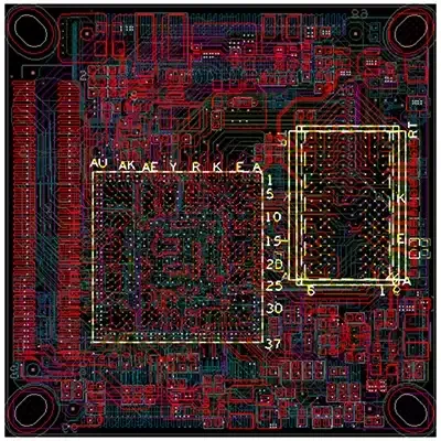
High-Speed Communication PCB Design
A PCB design profile for high-speed communication signals.
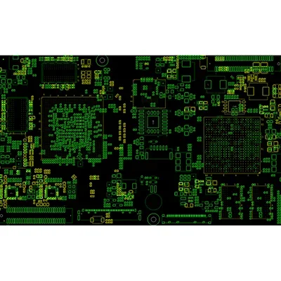
12-Layer Automotive High-Speed Backplane Design
A twelve-layer high-speed backplane design for automotive electronics.

High-Speed Server Backplane PCB Design
A high-speed backplane PCB design profile for server systems.
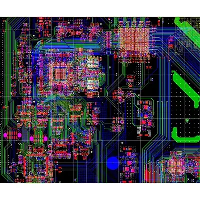
High-Speed High-Density PCBA Design
A PCB assembly design profile focused on high-speed signals and high-density layout.

AI Processing PCB Design
A PCB design profile for an artificial-intelligence computing application.
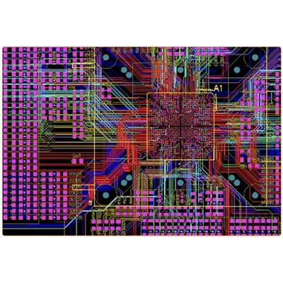
High-Frequency and High-Speed PCB Design
A PCB design profile combining high-frequency and high-speed design requirements.