4-Layer PCB Manufacturing
FLJ manufactures custom four-layer PCBs for prototypes and production. Choose the stackup, finished thickness, copper and surface finish for your circuit, with fabrication and controlled-impedance options for the build.
Four copper layers give a compact design more room for signal routing and reference planes. How those layers are assigned determines what the board can do with that space.
LAYERS
- 2 outer layers
- Component pads and routing
- 2 inner layers
- Assigned to the circuit
Layer roles and dielectric spacing are selected together.
Four Layers, Different Ways to Use Them
A four-layer PCB does not require one fixed arrangement of signal, ground and power. Two constructions illustrate the choices available when the outer surfaces carry components and routing.
Signal / Ground / Power / Signal
This arrangement reserves the two inner layers for ground and power distribution. The top routing layer is next to ground; the bottom routing layer is next to the power plane. That distinction matters when positioning fast signals and planning their return paths.
An internal power plane can distribute a supply across the board while leaving the outer copper available for routing. Multiple supply regions may divide that plane. A signal crossing the division no longer sees the same nearby reference copper, so its route needs to be considered together with the plane beneath it.
Signal + power / Ground / Ground / Signal + power
Two internal ground planes give each outer routing layer an adjacent ground reference. Power travels through traces or copper areas on the outside layers. That provides a useful alternative when both surfaces need ground-referenced routing and the power connections can fit alongside the signals and components.
The two ground layers still need appropriate connections. A signal moving from one outer face to the other also changes its nearest reference plane. The reference transition belongs in the layout, alongside the signal via.
Electrical assignments shown as examples. Copper and dielectric dimensions are not specified by these illustrations.
Choose the resources the circuit needs
The choice is where to allocate the available copper. A dedicated power plane provides distribution area; a second ground plane gives the two outer signal faces separate adjacent ground references. FLJ manufactures both arrangements, with the material and dielectric buildup selected for the circuit.
Specify the Finished Four-Layer Board
Material, dielectric spacing and copper specifications turn a layer assignment into a physical board. A finished board needs to fit both its electrical layout and the product’s mechanical assembly.
| Board option | Selection | Why it belongs in the build |
|---|---|---|
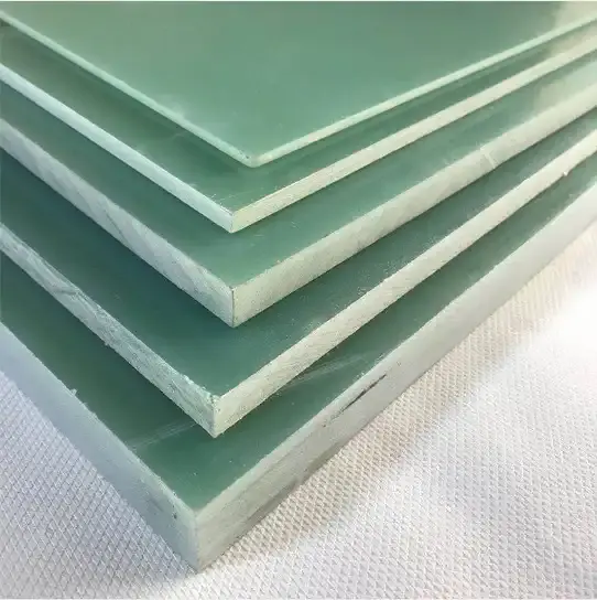
| Laminate | FR-4, high-Tg FR-4 and suitable specialty materials | Electrical and thermal properties, with a compatible bonding system |
| Finished thickness | The required board thickness and dielectric buildup | Connector fit, board support and signal-to-reference spacing |
| Copper | Inner copper and finished outer copper specified separately | Trace geometry, power distribution and the manufacturing buildup |
| Surface finish | ENIG, HASL or OSP, among the available finishes | Exposed-pad condition for soldering and the intended assembly |
| Delivery format | Individual boards or production panels | Handling, tooling and subsequent component assembly |
Total thickness is not reference spacing
The same overall board thickness can be divided differently between the core and the outer bonding layers. A thicker central core with thinner outer dielectric regions gives a different signal-to-reference distance from a construction with more evenly distributed spacing.
For a top-layer trace, H is the dielectric spacing to the adjacent reference copper. The full board thickness includes that region plus the core, the other dielectric layers and the conductors. Changing the central core thickness does not necessarily change H.
The selected dielectric properties, trace dimensions and surrounding copper form the impedance model. That is why a thickness label such as 1.6 mm needs its actual layer buildup before it can guide controlled-impedance routing.
Inner layers are patterned on the core before the stack is bonded. Outer copper can gain thickness through plating, which is why finished outer copper and inner copper remain separate specifications. FLJ can work from an existing stackup or build the four-layer construction around the stated thickness, copper and impedance needs.
Give Each Signal a Usable Reference
A route and the copper beneath it form part of the same electrical structure. A continuous reference plane lets the return current follow the signal’s path nearby. A gap in that plane changes the local environment even if the signal trace itself remains straight and unbroken.
What changes at a plane split
Before and after the gap, the trace has its nearby reference copper. Over the gap, fields and return current interact with the surrounding copper and potentially a more distant plane. That change can produce a local impedance discontinuity, reflections and a larger return loop.
The effect depends on the cross-section, gap geometry, signal edge rate and coupling. A differential pair is not automatically immune: imbalance can introduce common-mode current, which also needs a return path. The useful question is where the relevant return current can flow, not simply whether the net has electrical continuity.
Treat a layer change as a reference change
With two internal ground planes, a nearby ground connection can support return-current transfer when the signal changes sides. With ground and power as the two inner references, transfer involves coupling between the different networks. Ground stitching connects ground references; the power network remains electrically separate.
Plane continuity, a suitable reference transition and the trace’s dielectric geometry work together. Choosing them as part of the same four-layer construction keeps the signal route and its return path connected to the actual layout.
Match the impedance target to the actual geometry
A 50-ohm single-ended target or a differential target describes a transmission-line requirement, not a standard trace width for every four-layer board. Trace width and pair spacing need the actual dielectric spacing, copper and material properties. Surface copper near the trace can also change the field geometry.
Controlled-impedance fabrication uses the selected construction and its defined target. Applicable impedance measurements check the specified representative test structure; bare-board electrical testing checks the required connections and isolation. These are different checks, and neither alone establishes assembled-product EMC compliance.
A Practical Step Beyond Two Layers
| Choice | Where it fits | What the construction provides |
|---|---|---|
| Two copper layers | Connections and useful reference copper fit on two surfaces | A simpler laminate with routing and copper areas sharing the outside faces |
| Four copper layers | The circuit benefits from internal planes or additional routing space | Two more copper layers that can be assigned to the selected signal, ground and power arrangement |
For an embedded controller with several interfaces, this can mean keeping the component-facing surfaces available for connections while reserving inner copper for the selected planes. A mixed power-and-control circuit may instead prioritize where supply copper fits and how its switching paths relate to ground. The circuit’s actual connections determine the choice.
What changes in fabrication and cost
A conventional four-layer through-hole board can use an etched two-sided core, prepreg and outer copper foil bonded in one lamination cycle. Adding blind or buried connections may change the buildup and processing, depending on the construction. Extra processing is not always another lamination cycle.
Material, copper, hole geometry, board dimensions, finish and order quantity all influence the quotation. Four layers are a useful manufacturing option, not a fixed price category. Where more independent routing or plane space is needed, a six-layer construction may be a better fit than forcing the circuit into four layers.
Multilayer PCB manufacturing →Bare boards or a continued assembly build
FLJ supplies fabricated four-layer boards with inspection and electrical testing for the bare-board build. Controlled-impedance requirements carry through to the selected construction and test scope. Component sourcing, SMT and through-hole assembly are available when the order continues to a populated board.