
PCB Fabrication Equipment & Process Resources
Match the manufacturing route to the board you are designing. Our PCB scope connects materials, imaging, drilling, lamination, plating, finishing and verification for standard and specialized constructions.
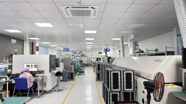
Equipment categories that shape PCB manufacturing
PCB fabrication turns the copper patterns and construction information in your design into a finished circuit board. Each process category controls a different part of the result, from layer alignment to hole connections and the finished outline.
The equipment route depends on the construction. A conventional multilayer FR4 board, a sequentially laminated HDI design and a metal-core board have different material and processing needs. We review those differences with the design rather than treating every published capability limit as one combined specification.
| Process category | Manufacturing task | Design information it connects with |
|---|---|---|
| Imaging and etching | Form the specified copper features | Trace geometry, copper weight and artwork |
| Lamination | Build the layered construction | Material selection and approved stack-up |
| Drilling | Create mechanical holes and applicable microvias | Hole sizes, via structure and board thickness |
| Plating and via processing | Establish interlayer connections and selected via structures | Aspect ratio, via fill and connection requirements |
| Mask and legend | Apply protective mask and component markings | Mask openings, color and legend data |
| Surface finish | Prepare exposed pads for the intended use | Soldering route and selected finish |
| Profiling and verification | Complete the outline and check the finished board | Dimensions, panelization and inspection scope |
Materials, stack-up and lamination
The stack-up connects the copper layers, cores and bonding materials with the desired board thickness and electrical performance. Material selection also affects thermal behavior, mechanical stability and the processing route.
Our published PCB scope includes FR4 multilayer, HDI, flexible, rigid-flex, RF, metal-core and ceramic constructions. For a special material or hybrid design, share the intended grade and stack-up so our engineering team can review the compatible construction and available manufacturing approach.
If the stack-up is still being developed, send the layer count and design goals. We can discuss material and construction options before the files are released.
Drilling and interlayer connections
Through-holes and vias connect the board’s layers and support inserted components. Hole diameter, board thickness, annular-ring geometry and the intended via structure all influence the drilling and plating route.
Mechanical drilling supports applicable through-hole and depth-controlled features. HDI constructions can use laser microvias where the material and structure support that process. Blind, buried and filled via designs are reviewed with the lamination sequence and connection requirements.
A drawing or marked-up view is useful when a feature needs explanation. Our team can help clarify the intended finished hole, via fill, back-drill or slot arrangement from the information you already have.
Copper features, mask and surface finishes
Imaging and etching establish the circuit geometry. The practical trace and spacing route depends on the selected copper thickness and construction, so fine-feature requests are reviewed together with the material and copper requirements.
Solder mask openings, legend placement and the selected surface finish complete the board for its intended assembly and use. The finish discussion can consider pad geometry, storage, soldering and contact requirements, including connectors or gold fingers where they are part of the design.
Our capability tables provide a starting point for comparing constructions. The final manufacturing specification connects the selected features with your actual board rather than combining separate process limits.
Finished-board verification and production review
The finished board is reviewed against the agreed drawing and acceptance plan. Dimensions, hole details, surface condition and electrical continuity or isolation address different aspects of board quality. Additional construction or impedance checks can be discussed where they are relevant to the order.
For supplier qualification, we can discuss the process categories and manufacturing questions that matter to your product. Send the Gerber package, board specification or preliminary construction details; our team will review them and follow up on open points.
A useful equipment conversation starts with the board: layer structure, material, copper, vias and the delivery stage. That provides more insight than a list of machine names without a defined manufacturing task.
Frequently asked questions
Can you review a specialized board construction?
Send the intended material, layer arrangement and special features. Our engineering team can review the manufacturing route and discuss suitable construction options.
Do all PCB materials use the same drilling process?
No. The material and via structure affect the available process. We review mechanical drilling, laser microvias and depth-controlled features against the specific construction.
What if my stack-up is not finalized?
You can send the layer count, available files and performance goals. We can begin the discussion and help clarify the construction details before production.
Explore related capabilities
Let’s review your next build
Send your available board files, drawings or project questions. Our team will review the information and follow up with you about the next step.