
ENEPIG PCB Manufacturing
Nickel–palladium–gold surfaces for soldering and specified wire-bonding pads.
FLJ manufactures ENEPIG-finished rigid boards, flex circuits and rigid-flex constructions. We build and specify each metal layer for the selected board construction and connection task.

Nickel, Palladium and Gold on the PCB Surface
FLJ supplies ENEPIG-finished boards with three distinct metal layers over the existing copper circuit: nickel, palladium and gold. Each layer contributes to the surface delivered for the selected connection task.

What the Palladium Layer Changes
In ENIG’s nickel-and-gold finish, the gold step acts on a nickel-based surface. ENEPIG first covers nickel with palladium, so the final gold forms over this intermediate metal. Palladium helps limit direct nickel attack during gold finishing; its coverage and condition depend on controlled chemical processing.
Separate Roles for Nickel, Palladium and Gold
Nickel, palladium and gold perform different jobs within the finish. Separate metal-layer callouts define the required amount of each material in the supplied surface.
| Finish layer | Function in the supplied surface |
|---|---|
| Nickel | Barrier between the copper circuit and outer finish, forming the base of the selected joining stack. |
| Palladium | Covers nickel before gold treatment and provides the intermediate surface for the final gold layer. |
| Gold | Thin outer surface protecting the prepared finish before soldering or the specified bonding operation. |
ENEPIG for Soldered and Wire-Bonded Connections
SMT and BGA Soldering Surfaces
The thin ENEPIG coating follows the formed copper pad geometry, preserving low-profile lands for the selected SMT or BGA build. FLJ can take finished boards into SMT assembly, including solder-paste printing, component placement and reflow with the chosen materials and thermal process.
During soldering, gold and palladium interact with the solder and can dissolve into it. The resulting joint therefore has an interface that differs from the as-finished gold surface. Coating amounts, solder alloy and thermal history determine how that interface develops, making the layer build part of the selected assembly process.
Pads for Specified Wire-Bonding Processes
FLJ fabricates ENEPIG-finished pads for the customer’s selected wire-bonding process. Wire material, bonding method and the supporting Ni/Pd/Au stack set the surface requirements. Finishing, cleaning and handling preserve the designated pad surface for that downstream operation; cleanliness, layer condition and thickness remain part of its process qualification.
The connection task also guides the alternative finish. ENIG provides a two-metal route for selected soldering builds; electrolytic soft- and hard-gold options serve specified bonding surfaces and repeated-contact wear duties.
How We Manufacture ENEPIG PCBs
Copper Preparation and Electroless Nickel
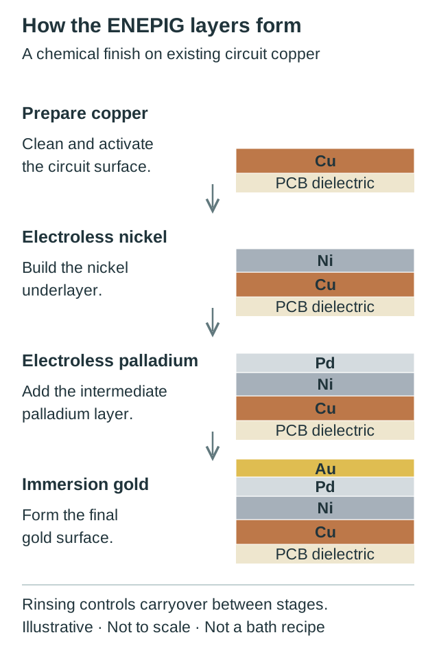
We begin with the exposed copper pads selected for ENEPIG. Cleaning removes contamination, while suitable microetching and activation prepare the copper for electroless nickel. The nickel layer forms over this prepared interface, so copper preparation contributes directly to adhesion and coating coverage.
The chemical route processes appropriately prepared isolated pads without a plating power feed. Treatment is directed to the exposed features prepared for the selected coating process.
Palladium Deposition Before Immersion Gold
We deposit palladium over the nickel before applying immersion gold. The palladium step produces the intermediate metal surface on which the final gold layer forms. Nickel surface condition influences palladium coverage, and the resulting palladium surface becomes the input to gold finishing. The selected chemistry and layer build are controlled at each stage.
Rinsing, Coverage and Layer Verification
Interstage rinsing limits solution carryover into the next bath and preserves the interface being formed. Final cleaning and drying prepare the finish for delivery and its intended soldering or bonding operation.
We check coating coverage and surface condition, with nickel, palladium and gold assessed against their separate layer callouts. Layer measurement addresses deposited metal; purpose-specific verification addresses the selected construction or joining requirement. The testing scope follows the product and connection process.