
PCB DFM & DFA Review Services
Find fabrication and assembly problems while the design can still be changed. FLJ reviews your PCB and PCBA data to identify manufacturing issues and recommend practical corrections before your next build.
A board can meet its electrical design rules and still need changes to a footprint, hole, solder-mask opening or panel. Our review connects those details with the processes used to fabricate and assemble your product, from prototypes to production.
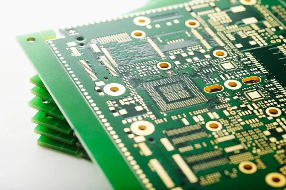
CAD rule checks and a manufacturing review work together. The rules configured in your design software can include fabrication and assembly constraints; an engineering review brings the selected materials, actual components and manufacturing route into the same discussion.
PCB Fabrication Review
The copper artwork, drill data, outline and fabrication notes describe different parts of the same board. A fabrication review checks how those features work together and how they will be produced.
Stackup, Materials and Copper
Layer construction influences both electrical behavior and fabrication. Material selection, dielectric thickness, copper weight and impedance requirements need to work as one stackup. We examine those relationships alongside the fine features in the layout.
Copper thickness also affects which trace widths and clearances can be made consistently. A layout developed for one copper weight may need adjustment when that construction changes. The review identifies where a different feature size or construction could make production more practical while retaining the intended circuit.
Holes, Vias and Board Features
A hole may connect layers, accept a component lead or secure the assembly mechanically. Its plating status, finished diameter and position should match that job. These details are checked against the drill information and drawing, including plated and non-plated features.
A connector lead must fit the finished hole after plating. The drilled opening and finished opening are different dimensions, because copper is deposited on the hole wall. Lead size, lead tolerance and finished-hole tolerance therefore belong in the same fit assessment.
The copper remaining around a drilled hole forms the annular ring. Its width matters when the drill position varies: enough copper must remain to preserve the connection to the pad and circuit. Clearance to neighboring conductors is checked at the same time. Slots, cutouts and board-edge features are also assessed against the intended finished geometry.
Solder Mask, Markings and Panel Layout
Solder-mask openings expose the intended solderable areas. An opening over an unintended copper feature, or mask covering part of a pad, can affect the later soldering operation. Reference markings, polarity indicators and fiducials also need to remain useful after the board is made.
Panel design connects fabrication with assembly. Rails provide handling space; fiducials provide registration references; tabs or scoring define how individual boards will be separated. We check these features against the populated board so an edge component does not occupy a clamp or cutting path.
PCB Assembly Review
Footprints and Part-to-Board Fit
A selected part has to match the board physically as well as electrically. Pin count, pitch, pad or hole geometry, and orientation are checked against the manufacturer’s package information. For example, a BOM may call for a leaded device while the layout uses a surface-mount footprint. The package and land pattern need to be reconciled before that part can be assembled.
We connect the selected package with its land pattern and assembly information, including pin 1 and polarity. Where a part or footprint needs to change, the finding identifies which relationship is wrong so the design can be corrected before the assembly is built.
Placement and Assembly Access
Parts need room for the operations around them. A narrow gap can obstruct a placement nozzle, soldering tool or rework operation even when the component bodies fit on the board. Component height and orientation also affect access and the selected soldering route.
For a wave-soldered assembly, placement also affects how solder reaches the joints. A larger part positioned ahead of smaller parts can shadow them from the wave. Orientation and spacing are therefore assessed for the soldering route, rather than treating every assembly as a reflow-only build.
Soldering and Inspection Considerations
Small chip components illustrate why a footprint review extends beyond matching the package outline. Different pad areas or copper connections can give the two ends different thermal responses during reflow. If solder wets the ends at different times, unbalanced forces can lift one termination and produce a tombstoned component. Pad geometry, connected copper and the soldering process are considered together.
An open via inside a solderable pad presents a different issue: solder can flow into the opening and reduce the material available for the joint. Moving the via or using a suitable filled and capped structure can address this during design review.
A tall neighboring component can obstruct an optical view of a joint; a BGA’s joints are hidden beneath the package itself. These different geometries inform the inspection plan. Contacts needed for programming or electrical tests are also identified during review, with the detailed methods carried into the PCB testing plan.
Review Findings and Recommended Design Changes
A useful finding connects a visible design detail to its manufacturing consequence. FLJ provides marked locations and engineering comments so your team can see what needs attention and why a change is recommended.
An Example: Unequal Copper Connections at a Chip Component
A · Broad copper connection
Compare its heat-transfer path with the other end.
B · Narrow trace connection
Review the two ends as one soldering problem.
Finding: One pad connects directly to a broad copper area; the other connects through a narrow trace.
Manufacturing effect: The two ends can respond differently to the reflow profile, increasing the possibility of uneven wetting and a lifted termination.
Recommended change: Review the paired land geometry and copper connections for a more balanced response, while preserving the circuit’s current-carrying and heat-transfer needs. The component’s recommended footprint and the soldering process guide the final change.
Each finding is tied to the relevant board location, BOM reference or drawing note. If a correction changes a specified material, stackup, footprint or layout feature, we confirm it with your team and check the revised data before production.