
AOI & SPI Inspection Services
3D paste inspection before placement. Optical inspection of the assembled board.
FLJ provides AOI and 3D SPI within PCB assembly, connecting inspection findings with the relevant printing, placement and soldering work.
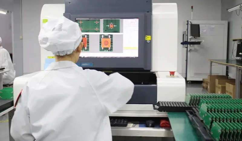
SPI and AOI at Different Stages of PCB Assembly
FLJ provides 3D solder paste inspection (SPI) and automated optical inspection (AOI) within PCBA manufacturing. SPI checks printed solder paste before component placement; AOI evaluates visible component and solder-joint features at a selected assembly inspection point.
- PrintStencil printing
- Inspect paste3D SPI
- PlaceComponent placement
- SolderReflow
- Inspect assemblyAOI
| Feature | 3D SPI | AOI |
|---|---|---|
| Stage | After solder paste printing, before placement | At a selected assembly inspection point after reflow |
| Object | Solder paste deposited on board pads | Visible components and solder-joint features on the assembled board |
| Observation | Paste volume, height, area and position | Component presence, alignment, visible orientation or markings, and solder-joint appearance |
| Manufacturing focus | Check the relevant print registration or deposit setup | Review the indicated component or joint and the relevant assembly operation |
The inspected object changes as the board moves through assembly. SPI sees the printed deposits before parts cover them; AOI sees the component and solder features available to the camera after assembly. The two checkpoints therefore support different manufacturing decisions.
3D Solder Paste Inspection Before Placement

Paste Volume, Height, Area and Position
FLJ uses 3D SPI to measure the printed deposits before placing components. Several quantities describe the print because paste geometry and pad alignment provide different information:
| Measurement | What it describes |
|---|---|
| Height | How far the deposit rises above the board surface. |
| Area | The surface area covered by the paste. |
| Volume | The total amount of paste in the deposit. |
| Position | How the deposit aligns with its pad or intended location. |
Height alone does not establish how much paste is present. Deposits with the same height can cover different areas and contain different volumes. Reading geometry and alignment separately helps distinguish an amount or shape difference from a registration error. These measurements describe printed paste before reflow; placement and soldering then shape the finished joint.
Addressing Print Issues While Deposits Are Accessible
We check a flagged deposit against its pad and the intended print while the paste remains accessible. An offset directs attention to registration in the stencil-printing process; an amount or shape difference directs attention to the stencil condition and deposit setup. We investigate the relevant print condition and reinspect the affected print after an appropriate correction.
Automated Optical Inspection of the Assembled Board
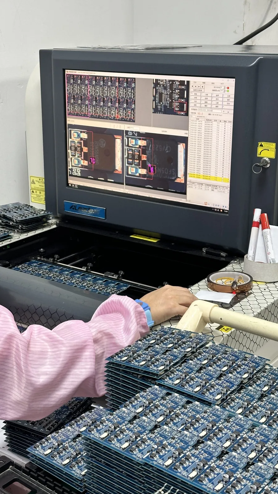
After component placement and soldering, FLJ uses automated optical inspection (AOI) to examine visible features on the assembled PCBA. This checkpoint focuses on the mounted components and their visible solder joints, so the inspection can compare assembly results with the intended board layout.
Component and Visible Solder Features
AOI images can be configured to check whether expected components are present, whether their positions align with the board layout, and whether visible orientation marks or polarity indicators face the intended direction. The same images can show visible solder-joint features for comparison. These observations connect the inspection to specific assembly details: a missing or shifted component changes what appears at its expected position, while a reversed mark or an unusual visible joint changes the feature the program evaluates.
Lighting, Programmed Comparison and Review
Camera Access
The features available to the camera depend on the board geometry and the inspection setup. A tall component can block light or obscure a nearby low-profile part or joint, so the lighting and viewing direction need to make the target feature visible. AOI evaluates the image of an accessible surface; a joint hidden beneath a package is not represented by an outside view of that package.
Programmed Reference
Lighting and camera angle shape how component edges, markings and solder surfaces appear in the captured image. With a usable view of the feature, the AOI program compares its observed position or appearance against product-specific reference information. That reference can come from board design data or a suitable approved sample; a first board does not become an acceptance standard simply because it was inspected first.
Review of Findings
The comparison directs attention to locations where the image differs from the programmed reference. A difference identifies a position for review, while the visible feature and the product requirements determine whether it reflects an assembly issue or an acceptable variation. This keeps AOI findings tied to an identifiable component, marking or visible joint on the board.
From Inspection Findings to Verified Assembly
An SPI or AOI alert identifies a location and feature for review; it does not by itself confirm a defect. The technician checks the marked area against the intended paste deposit, component position, or visible solder connection, then routes a confirmed issue to the manufacturing step that produced it. This keeps an observed difference tied to the right assembly object before any correction is made.
A paste-volume or position finding leads back to printing: the print setup or process is corrected as appropriate, and the affected deposit is measured again before placement proceeds. A component-position finding leads to a placement correction, followed by a check of that component’s location and orientation. A concern on a soldered connection is reviewed in the context of the soldering work; any applicable correction is followed by reinspection of the affected joint or visible feature. The recheck addresses the feature involved and does not replace other inspection or testing selected for the order.
Some assembly connections are hidden from a surface camera. For a selected hidden-joint concern, X-ray inspection provides an image of the internal connection for review; that image does not establish electrical continuity or prove product operation. Electrical measurement checks accessible electrical behavior, while functional verification applies power and, where the product requires it, firmware or interface conditions to compare the response with its expected behavior. These are distinct checks for distinct questions, as described in product verification.
For an order that includes documented results, FLJ supplies the specified inspection and test records. The record scope identifies the checks and results to accompany the assembly, so the delivered information matches the verification included in the order.
Inspection within your PCBA order
Send your assembly requirements for a build that includes the relevant inspection and product verification.