
Side plating · Selected outer and inner contours
Edge Plating PCB Manufacturing
Conductive board edges for grounding, shielding and assembly interfaces.
FLJ manufactures edge-plated PCBs with copper metallization on selected outer profiles and internal cutouts. The plated wall, its connections to the circuit and the finished panel are built together through the fabrication route, from prototypes to production.
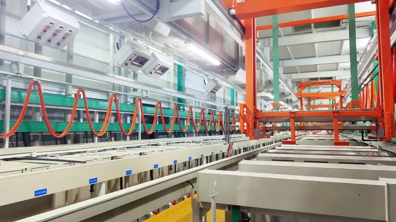
The sidewall becomes part of the circuit
Edge-Plated PCB Constructions
Outer Profiles and Internal Cutouts
Edge plating creates a conductive wall through the board thickness at the specified contour. It can run along selected portions of the external profile or around selected walls of an internal cutout. Copper on the board faces and designated inner layers connects that wall to the intended circuit.
Coverage can follow a chosen edge segment or a series of separate regions. The outline drawing identifies the plated spans, while the layer data defines where they connect. An ordinary routed cutout and a metallized cutout therefore require different fabrication treatment.

Grounding, Shielding and Edge Assembly
- Grounding & shielding
- A metal boundary connected to the assigned reference copper can become part of the board’s shielding arrangement. Its continuity and connection to the rest of the assembly determine how that boundary works.
- Housing connections
- An accessible plated edge provides a defined contact region at the board perimeter. The contact location, surface finish and enclosure interface are considered together.
- Soldered edge interfaces
- Specified edge regions can provide a solderable connection to another part of the assembly. The mating surface and assembly access determine the usable plated span.
For discrete recessed solder contacts, see castellated PCBs. A removable socket connection uses gold finger contacts on the board faces. Edge plating provides the conductive wall at the contour.
Expose the surface before building the metal
Manufacturing the Conductive Edge
The required wall has to be accessible when metallization takes place. FLJ incorporates the selected routed regions, layer connections and panel supports into the production design before that stage.
Pre-Routing and Sidewall Preparation
The contours intended for plating are routed while the board remains supported in the production panel. This exposes the laminate wall and the copper features that are to join the plated edge.
Wall preparation removes machining residue and burrs so that copper can be formed on the intended surface. The tool path and the condition of the exposed edge both affect the surface available for metallization.
Copper Metallization and Surface Finish
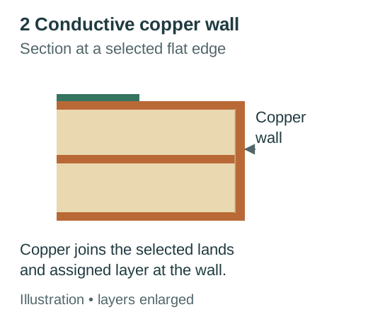
The prepared dielectric first receives a conductive starting layer. Copper is then built up by electroplating over that surface, forming the specified wall coating and joining it to the assigned lands and layers. This copper construction is completed before the final surface finish is applied.
The selected finish protects the exposed copper and provides the surface required for the intended contact or soldering operation. Wall copper, face-layer copper and the final surface treatment have separate specifications.
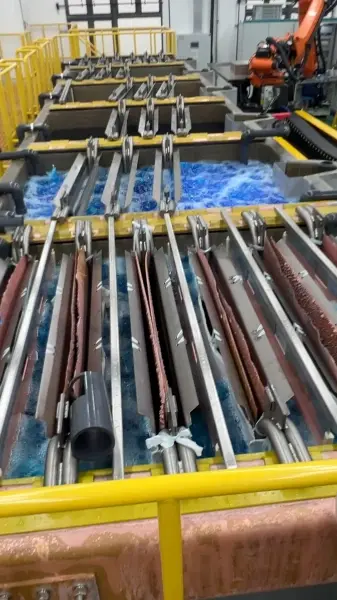


ENIG is an available finish for edge-plated constructions. The board faces, exposed wall and any areas requiring solder-mask coverage are defined for the build. Our PCB surface finishes page explains the wider finish choices and their roles in assembly and contact performance.
One contour, different copper relationships
Layer Connections and Edge-Plating Geometry
The intended edge is the common reference for the copper pattern. Connected copper reaches the wall; isolated copper stops short of it. These relationships determine which nets become part of the plated boundary.
Connected Lands and Selected Inner Layers
Face lands provide copper beside the edge, and a designated inner layer can connect directly to the wall. The fabrication data names these layers and their electrical connections.
Other layers keep the required separation from that boundary. An inner power plane or signal conductor is connected to the edge only when the design assigns it there. The layer pattern must preserve isolation for the other nets.
Artwork Overlap and Copper Keepouts
The copper artwork can extend across the intended contour to define the region to be metallized. That extension is a manufacturing instruction relative to the profile. It is separate from the copper retained inside the finished board and from the setback of copper that must remain isolated.
The section uses one contour datum for A, B and C. The artwork allowance extends outward; the connected land and isolated-copper setback are measured inward. The finished board keeps the defined land and wall, while the outward extension remains part of the fabrication artwork.
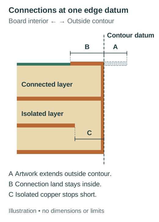
A, B and C describe the layout around the contour. The overall board/profile dimension must state its finished condition, including deposited metal where that finished surface is the acceptance boundary.
Scroll to compare each object, reference and manufacturing purpose →
| Geometry object | Reference and direction | Manufacturing purpose |
|---|---|---|
| A · Artwork extension | Outward from the intended contour in the copper artwork. | Defines the metallization region across the outline. |
| B · Retained connected copper | Inward from the contour to the end of the retained connection land. | Provides copper inside the board that joins the wall. |
| C · Isolated-copper setback | Inward from the contour to the nearest non-connected copper. | Keeps the specified conductor separate from the plated boundary. |
| Edge-wall copper thickness | Through the deposited wall copper, specified in µm. | Defines wall copper separately from face-layer weight in oz and the final surface finish. |
The illustration identifies measurement objects and directions; it does not set numerical manufacturing limits. The plated spans, layer connections and clearances are brought together in our PCB fabrication review.
Coverage follows the accessible contour
Panel Support, Separation and Finished-Edge Checks
Plated Spans and Support Interruptions
A support bridge keeps the board joined to its panel during processing. At that bridge, the laminate is still connected, so the region is not exposed as a free sidewall during metallization. Removing the bridge later exposes a new edge. In the illustrated route, this leaves an unplated interruption between the previously plated spans.
The panel arrangement places those interruptions in relation to the required housing, ground or solder-contact regions. A request for a continuous plated boundary therefore needs a support and separation route that preserves that coverage. A score-created edge is considered with its timing in the process, because a surface exposed after metallization has not received the earlier wall treatment.
Checking Coverage and Electrical Connections
Finished-edge checks examine the defined plated spans, exposed-wall condition and final profile after separation. Copper coverage and surface treatment are examined at the regions called out for the build, alongside any specified wall-thickness or adhesion verification.
PCB electrical testing checks the intended conductive networks and isolation. Wall coverage, coating thickness and the physical contact surface remain separate inspection objects. A shielding or enclosure interface is then assessed within its finished assembly.

Specify the edge your assembly needs.
Boards can be supplied in the specified production panel or as separated parts, with plated spans and release locations identified for the finished edge. Send the marked contours, connected layers and nets, and wall/finish requirements for a matching FLJ fabrication quote.