

Controlled-depth PCB fabrication
Backdrill PCB
Manufacturing
Remove the unused copper.
Keep the connection your circuit needs.
FLJ manufactures multilayer PCBs with controlled-depth backdrilling for high-speed interconnections. Single-sided and double-sided machining remove unused plated barrel sections while preserving the functional connection, from prototype boards to production.
Get a backdrilled PCB quoteSingle-sided and double-sided backdrilling
Backdrilling Services for High-Speed PCBs
Via Stubs and the Signal Path
A plated through-hole can carry a signal from the board surface to an inner-layer land, while its copper wall continues beyond that connection. The unused extension is a via stub. It remains attached to the signal path even though it does not carry the connection to another required land.
At the junction, some signal energy can enter this branch and return as a reflection from its open end. The returning energy can alter the waveform and timing margin at the receiver. Stub length and the signal’s frequency content influence that behavior.
Backdrilling removes much of the unused copper extension. It addresses this local discontinuity within a larger high-speed PCB construction, where routing, reference planes, materials and connectors also determine channel behavior. Backplanes, networking boards and dense board-to-board interconnects are common settings for that combination.
Single-Sided and Double-Sided Backdrilling
The entry face follows the copper that is to be removed. A surface-to-inner-layer connection may leave a stub toward the opposite face. An internal-to-internal connection can leave unused copper toward both surfaces, requiring two separate cuts.
Each cut stops short of the last required connection, leaving a controlled residual stub. The aim is to reduce the unused extension while retaining the copper at the functional land. A double-sided construction has a separate machining direction and stopping position for each face.
Z depth · XY registration · Copper envelope
Depth, Residual Stub and Copper Clearance
The backdrilled feature is defined by where the cutter enters, how far it travels and how its removal envelope sits around the original plated hole.
Drilling Depth and the Remaining Stub
The machining program sets travel from the entry reference to a defined tool position. In the illustrated example, that position is the drill-tip apex. Residual stub length describes the copper left beyond the last functional connection: it is assessed at the barrel wall, rather than at the center of the drilled cavity.
The actual layer position, board thickness and tool-tip shape influence the relationship between them. A conical tip reaches farther at the hole center than at the original barrel wall. The copper remaining at that wall is therefore not identified by the position of the drill apex alone.
Published process reference. Residual stub targets and depth tolerance follow the selected board construction.
PCB fabrication capabilitiesCutter Diameter and Hole Registration
The secondary cutter is larger than the original plated hole so its cutting envelope can clear the barrel wall. Its diameter and position must work together: a cut that misses part of the wall can leave an unwanted copper crescent.
A larger removal envelope also occupies space around the original hole. Adjacent traces, planes and lands need clearance from that envelope throughout the machined span. Registration allowance and nearby copper therefore belong in the same geometric decision.
Where the layout instead calls for a connection confined to selected layers, blind and buried via constructions provide a different fabrication route. The choice follows the layer access, routing space and complete board construction.
A backdrill definition connects these dimensions to the same selected hole and connection:
Scroll to view each feature and its relationship →
| Feature | Relationship in the board | What it defines |
|---|---|---|
| Entry face & retained layer | The side of the unused extension relative to the required connection | Machining direction and retained span |
| Depth & tool-tip envelope | Commanded travel and the cutting shape relative to the actual connected layer | The machining position |
| Residual stub & retained land | Unused copper extending beyond the last required connection | The finished copper length to be checked |
| Cutter diameter & registration | Removal envelope around the original plated wall | Copper removal and surrounding clearance |
Making the specified removal span
Controlled-Depth Backdrilling in Manufacture
From Plated Through-Hole to Secondary Cut
Backdrilling acts on an existing conductive barrel. Primary drilling, hole-wall preparation and copper metallization establish the plated connection first. The secondary cut then removes the part of that wall which lies outside the required electrical span.
FLJ prepares the machining data around the selected holes, entry faces, retained layers and cutter sizes. Holes sharing a removal depth can be organized into machining groups, while connections at different layers require their own stopping positions. For two-sided work, each face has its corresponding reference and removal span.
The machining operation is registered to the original hole pattern. The programmed cut combines the layer-position information with the cutter’s geometry, so the intended copper is removed without cutting through the required connection.
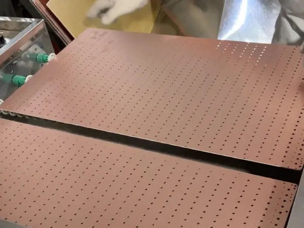
Machining and process control
Manufacturing Controls for Backdrilled PCBs
Panel Support & Depth Referencing
FLJ sets up panel support and the entry reference for controlled-depth machining. Local board shape, thickness variation and the connected layer’s position affect how the programmed travel corresponds to the physical board.
Tool Registration & Chip Removal
The cutter is aligned with the original hole pattern. Tool condition, spindle behavior and chip evacuation are controlled during removal of the copper and laminate; these factors affect the cavity and the copper remaining around it.
Cleaning & Connection Checks
After cutting, the opening is cleaned and examined for retained chips and incomplete removal. The retained connection is assessed alongside the machined region, with sampled sections used to examine the remaining copper.
A sampled section can reveal an excessive residual length or copper remaining on one side of the cavity. Excess residual length directs attention to the depth reference and layer/tool geometry; a localized copper remnant directs attention to cutter coverage and registration. An electrical pass alone does not establish that the removal geometry is complete.
Observe the copper that remains
Verifying the Backdrilled Connection
Residual Copper and the Retained Connection
A prepared microsection exposes the cut cavity, the end of the remaining barrel and the connection at the retained layer. These features show whether the intended copper was removed and where the residual stub ends relative to the functional land.
The section needs to pass through the feature being assessed. Its position and preparation affect what is visible; an off-center section can give a misleading view of the drilled cavity. The result describes the sampled plane rather than every location in every hole.
Geometrical and Electrical Checks
Bare-board electrical testing checks the continuity and isolation of the copper network. A connection can pass that test while still retaining an unwanted stub, so electrical connectivity and residual geometry are separate inspection questions.
Signal-integrity evaluation considers the wider channel response, including the via transition. A line-impedance coupon and its TDR result describe their tested structure; they do not automatically report the residual copper length of every backdrilled connection.
Manufacture your backdrilled PCB
Send the fabrication data, stackup and quantity, with the selected backdrill holes, entry faces, retained layers and residual-stub requirements. FLJ connects that definition with PCB fabrication and controlled-depth machining.