
Rigid PCB Manufacturing
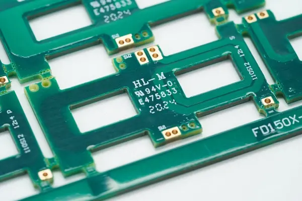
FLJ manufactures rigid printed circuit boards for prototypes and production. From straightforward single-sided boards to multilayer constructions, we build the copper connections, plated holes and finished board geometry that your assembly needs.
Rigid PCB Options
A rigid PCB provides a solid platform for copper circuitry and mounted components. Its laminate structure supports a defined board shape and component position. FR4 is a common material choice; rigid describes the board’s structure rather than one particular laminate grade.
Standard and high-Tg FR4, low-loss and RF laminates serve different electrical and thermal needs. Material selection follows those needs alongside the layer construction; a material family name alone does not define the complete board.
Materials and stackups →Rigid PCB Manufacturing Capabilities
These selected FLJ process references help establish the fabrication scope. The complete manufacturing-capability page provides the wider tables and construction-specific detail.
Complete manufacturing capabilities →Have a board drawing ready?
Send your fabrication enquiry →| Feature | FLJ process reference | Application context |
|---|---|---|
| General rigid-board layers | 1–30 layers | Single-sided through multilayer constructions |
| Finished copper | Outer up to 8 oz; inner up to 6 oz | Copper weight affects trace width and spacing |
| Mechanical finished holes | 0.10–6.2 mm | Finished opening and drill diameter are different |
| Finished thickness tolerance | ±0.1 mm at ≤1.0 mm; ±10% above 1.0 mm | Match finished thickness to mechanical fit |
| Maximum finished size, 2–20 layers | 533.4 × 838.2 mm / 21 × 33 in | Applies to this stated layer range |
| Surface finishes | ENIG, lead-free HASL, OSP, immersion tin/silver and plated gold | Select for soldering or contact requirements |
These references describe different manufacturing conditions, rather than one construction combining every minimum and maximum. The approved stackup and drawing define the board to be produced.
Thickness, Shape and Assembly Fit
The finished PCB has to fit the product around it. Board thickness can determine how an edge connector mates, how a board sits in a guide or slot, and how much room remains for nearby components. Nominal thickness and its tolerance therefore belong with the mechanical design. Using FLJ’s general ±10% reference for a board above 1.0 mm, a nominal 1.6 mm thickness corresponds to 1.44–1.76 mm. This illustrates the stated tolerance; a mating slot or connector needs to accommodate the actual specified range.
Thickness Comes from the Construction
Copper, cores and bonding layers contribute to a multilayer board’s final thickness. Prepreg flows and cures during pressing, so the construction needs to be assessed as a finished stackup. Changing the material or copper can affect more than the drawing’s nominal thickness.
Profiles, Slots and Mounting Holes
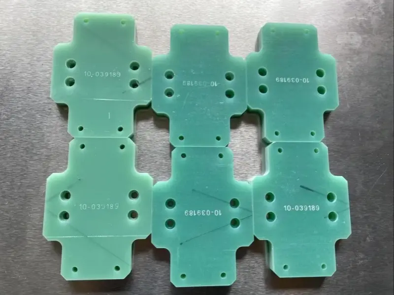
A routed outline, internal cutout and mounting hole perform different jobs in the assembly. Their positions define clearances, fastener locations and how the board is supported. FLJ manufactures these features from the board geometry and drill information, with plated and non-plated features identified separately.
Delivery as individual boards or a panel also affects the edge condition. Routed tabs and V-scoring create different separation paths; the panel arrangement should leave the component and mechanical areas needed for assembly and separation.
Flatness During Manufacturing and Assembly
Rigid does not mean immune to deformation. The laminate combines copper, resin and glass reinforcement, and its response to heating depends on the materials, construction and thermal history. Uneven copper distribution or an unbalanced stack can contribute to distortion.
Large openings and long unsupported sections can also change how a board carries its own weight or assembly loads. Such movement can alter component placement height, soldering contact and how a finished board sits in its housing. FLJ considers board support, layer construction and copper distribution together with the required finished geometry.
How the Rigid Board Takes Shape
Fabrication turns the design data into connected copper layers, protected surfaces and a finished mechanical outline. The route follows the chosen construction.
Copper Patterns and Layer Bonding
Copper is imaged and etched to form the required conductors. For multilayer boards, prepared inner cores are aligned with the bonding layers and copper foil, then laminated under controlled heat and pressure. Layer registration keeps internal features aligned with the later holes and outer patterns.
Holes and Interlayer Connections
Drilling creates the required openings. Metallization and copper plating form conductive hole walls where electrical connections are needed. Imaging, plating and etching follow the selected process route to form the outer conductors and their connections. Non-plated holes retain their specified mechanical role.
Protected Surfaces and Exposed Contacts
Solder mask covers the intended copper areas while leaving specified pads and contacts accessible. Surface finishing treats the exposed copper for its later use. Solder mask and surface finish are different parts of the board, with different functions.
Finished Profile and Board Separation
Routing, slots, scoring and any specified edge work create the final board form or its panel arrangement. For an edge connector, details such as the contact finish and bevel belong with the mating geometry, rather than being treated as decorative features.
Board Features and Verification
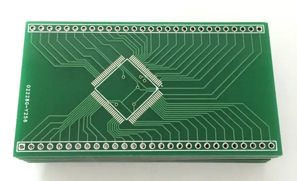
Copper thickness, conductor geometry and insulation spacing shape the board’s electrical and manufacturing requirements. A heavier copper construction needs suitable routing dimensions; adding copper weight is not a universal substitute for designing the current path and heat flow.
A component lead must fit the finished plated hole. Copper deposited on the hole wall changes the opening from its drilled size, so lead dimensions, finished-hole tolerance and the intended soldering arrangement need to be considered together. A mounting hole has a different purpose, and its plating status follows the mechanical or grounding design.
Dimensional checks address the finished outline, thickness and relevant hole locations. These checks connect the physical board with the fabrication drawing and the fit needed in the product.
Copper-pattern inspection and bare-board electrical testing address a different question: whether the fabricated connections and isolation match the circuit data. FLJ’s PCB testing page explains the available methods. Assembly inspection and powered functional testing address the later populated board.
Where Rigid PCBs Fit
Control and Interface Electronics
A fixed mounting arrangement can bring connectors, indicators and control circuitry onto a stable board platform. The outline and connector positions connect the electrical design with the enclosure and panel.
Power and Industrial Hardware
Copper construction, insulation and mounting features can be selected around power paths and thermal needs. A suitable current path, cooling arrangement and electrical clearances give that construction its purpose in the product.
Computing and Communications
Multilayer constructions provide space for routing and reference planes. Signal requirements can influence dielectric selection, stackup, controlled impedance and the choice of via structures. Detailed high-speed, RF and HDI options are covered on their dedicated pages.
Rigid PCB Questions
Can a Rigid PCB Be Bent to Fit an Enclosure?
A conventional rigid board is not designed as a bendable interconnect. If the product needs a folded connection or movement, a flexible, rigid-flex or suitable semi-flex construction may be more appropriate. FLJ’s board-family pages explain those different structures.
Do Mounting Holes Need Plating?
That depends on their role. A hole used only for mechanical attachment and one intended to provide an electrical connection can require different treatment. The drawing and connection design identify which holes are plated and which remain non-plated.