
SPECIALTY LAMINATES · FINISHED CIRCUIT BOARDS
Rogers PCB
Manufacturing
RO4000, RO3000 and RT/duroid boards for your RF hardware.
FLJ manufactures double-sided, multilayer and mixed-material PCBs using Rogers laminates. Choose RO4000, RO3000 or RT/duroid constructions for antenna circuits, RF modules and boards that combine radio-frequency performance with power and control electronics.
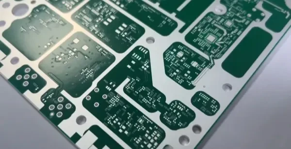
MATERIALS THAT SHAPE THE PRODUCT
Rogers PCB Products and Material Options
Rogers is a family of materials, with distinct resin systems and product grades. The selected grade, dielectric thickness and copper foil define the starting construction of your board.
RO4003C
A glass-reinforced hydrocarbon/ceramic laminate for RF feed networks, filters and microwave circuits. Its low dielectric loss combines with processing similar to epoxy/glass laminates, making it a practical option for multilayer RF boards.
Lower published Df than RO4350B; not UL 94 V-0 rated.
RO4350B
A flame-retardant RO4000 grade for RF boards with a UL 94 V-0 material requirement. It supports plated-through-hole and multilayer constructions, including boards integrating RF circuits, power distribution and digital control.
A different dielectric and thermal profile from RO4003C.
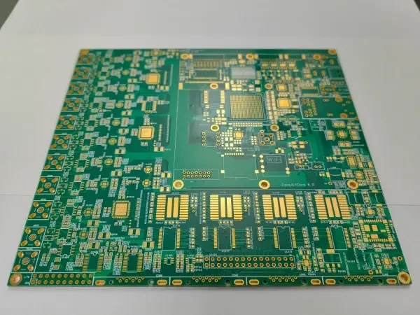
PTFE-BASED MICROWAVE MATERIALS
RO3003
A ceramic-filled PTFE laminate for microwave circuitry, patch antennas and phase-sensitive networks. Its material system brings low dielectric loss together with dimensional and electrical characteristics suited to multilayer and hybrid boards.
RT/duroid 5880
A glass-microfiber-reinforced PTFE composite for low-loss microwave and broadband circuits. Its low Dk offers another construction option for antenna elements and transmission structures, with foil and thickness selected for the circuit.
| Grade | Process Dk | Typical Df at 10 GHz | Material system |
|---|---|---|---|
| RO4003C | 3.38 ± 0.05 | 0.0027 | Hydrocarbon / ceramic, glass reinforced |
| RO4350B | 3.48 ± 0.05 | 0.0037 | Hydrocarbon / ceramic, glass reinforced |
| RO3003 | 3.00 ± 0.04 | 0.0010 | Ceramic-filled PTFE |
| RT/duroid 5880 | 2.20 ± 0.02 | 0.0009 | PTFE, glass microfiber reinforced |
Material values describe laminate properties, not finished-board insertion loss. Process Dk and design Dk can differ. Sources: RO4003C / RO4350B, RO3000 data sheet, RT/duroid 5880.
MATERIAL-SPECIFIC FABRICATION
How We Manufacture Rogers PCBs
The resin, reinforcement and copper construction determine how the laminate responds to cutting, wet processing and heat. RO4000 and PTFE-based materials follow different preparation routes.
Imaging and etched copper
We image the circuit pattern onto copper-clad material and etch the conductors, pads and clearances. Artwork compensation accounts for copper removal so the finished trace and gap reflect the intended RF geometry. Foil profile, copper thickness and conductor shape remain part of the electrical construction.
Optical inspection checks the circuit features before inner layers are enclosed or the board advances to finishing.
Drilling through different materials
Mechanical drilling produces component holes and interlayer connections. PTFE can soften around the tool and produce debris that adheres to the hole wall. Drill condition, chip removal and panel support help preserve the bore and exposed inner-layer copper.
In a hybrid panel, softened PTFE chips can travel along the bore as they are evacuated toward the entry side. We plan material orientation and chip removal together to reduce deposits at inner-layer copper interfaces.
Hole preparation and copper plating
RO4000 laminates support a processing approach similar to epoxy/glass. PTFE surfaces require a preparation route suited to their low chemical reactivity. Conventional epoxy desmear chemistry does not remove PTFE in the same way and may attack fillers in ceramic-filled grades.
Cleaning exposes the inner-layer copper; suitable activation prepares the dielectric surface for copper adhesion. A conductive seed layer then supports electroplating through the bore. Cross-sections inspect the plated barrel and its junctions with the internal copper.
Pressing, finishing and electrical checks
Multilayer fabrication joins patterned cores with the selected bonding material. Registration, copper distribution and resin flow contribute to the final layer alignment and dielectric spacing. Surface finish and solder mask complete the exposed pad and conductor areas, followed by profile machining.
Electrical testing checks for opens and shorts. Controlled-impedance builds include the specified coupon measurement alongside dimensional and visual inspection.
Need more detail on RF circuit features? Explore RF and microwave PCB fabrication
ONE BOARD · DIFFERENT LAYER FUNCTIONS
All-Rogers and Rogers / FR-4 Hybrid PCBs
An all-Rogers construction places the selected specialty materials throughout the dielectric stack. A hybrid construction uses Rogers laminate on RF-critical layers and a compatible FR-4 system for control, power or other supporting layers.
The bonding material connects these cores into one multilayer board. Its flow and cure behavior must suit both material systems and fill around the patterned copper. PTFE fusion bonding is a different process: using PTFE itself as the bonding layer can require temperatures that most FR-4 cores cannot tolerate.
The cured bonding layers also form part of the dielectric spacing between conductors. We account for their thickness alongside the core thickness, copper distribution and layer alignment during lamination. Plated through holes then connect the chosen layers across the mixed-material stack.
Hybrid fabrication can reduce specialty-laminate use. Total price also reflects bonding materials, lamination work, material availability and panel utilization.
A hybrid board, layer by layer
Example material arrangement · six copper layers
Core and bonding thicknesses both contribute to the finished dielectric construction.
FROM MATERIAL TO HARDWARE
Rogers Boards for RF Products
Our boards support antenna and microwave circuitry as well as mixed RF/control assemblies. Material selection follows the loss, phase, thermal and construction needs of the actual circuit.
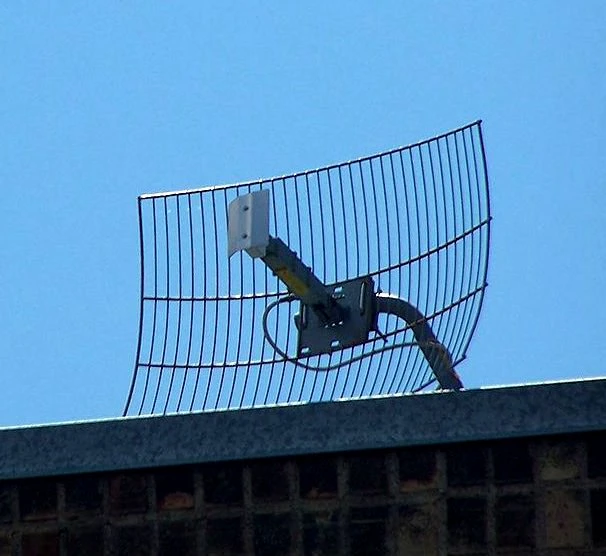
Antennas and wireless links
Feed networks, filters and RF front ends use low-loss laminates to carry signals between components and antenna interfaces. Single-core boards and multilayer constructions serve different circuit integration needs.
Radar and compact RF modules
Dense RF products combine microwave circuitry with bias, control and processing. Rogers and hybrid boards provide material and interconnect options for this integration, with manufacturing carried through to PCB assembly when required.
Application photographs illustrate hardware categories; they are not FLJ customer projects or identification of the laminates inside the pictured products.
PROTOTYPE TO PRODUCTION
Order the Rogers Construction Your Design Uses
FLJ supplies prototype and production boards with the selected laminate grade, dielectric thickness, foil option and bonding system carried into the fabrication record. Purchased-material and lot references stay linked to the board revision. Repeat builds retain the released construction; a proposed material alternate is assessed against that construction before substitution.
Material availability, copper configuration, layer count and panel use affect both purchasing and fabrication cost. A quote for your actual board is more useful than a fixed price multiplier attached to a material name.
Request a Rogers PCB quote
Send the fabrication files, stackup, named Rogers grade, quantity and any impedance or assembly requirements. Include the preferred material thickness and copper option if already selected.
Discuss Your Rogers PCBHave a laminate grade beyond these examples? Include the full product name in your enquiry.