PCB design
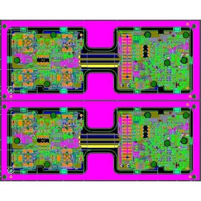
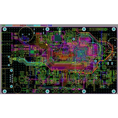
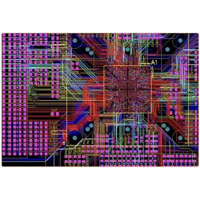
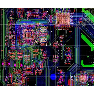
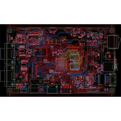
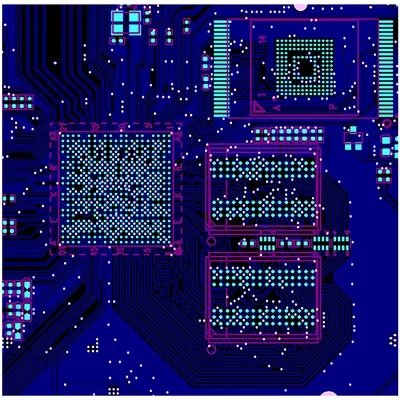
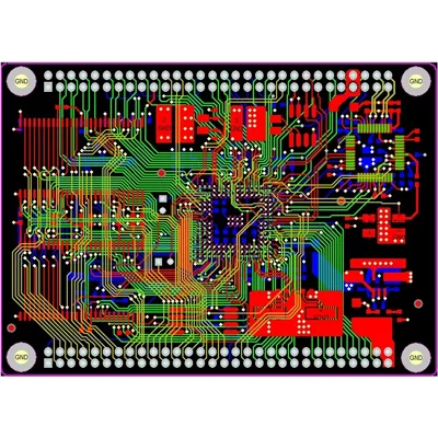
4-Layer HDI Switch PCB Design
A four-layer HDI PCB design for a switching-circuit application.
 FLJ PCBManufacturing your next idea
Explore circuit boards, control electronics and PCB designs across applications. Find a product close to your requirements and discuss the next build with our team.
A four-layer HDI PCB design for a switching-circuit application.
A PCB design profile combining high-frequency and high-speed design requirements.
A PCB assembly design profile focused on high-speed signals and high-density layout.
An any-layer HDI PCB design profile for dense interconnection requirements.
A ten-layer PCB design using a two-stage HDI structure.
A sixteen-layer PCB design with a two-stage HDI structure.
An eight-layer PCB design using a two-stage HDI structure.
Share your board, design files or project requirements with our engineering team.
FLJ PCBManufacturing your next ideaShenzhen Philifast Electron Co., Ltd.
PCB manufacturing, assembly and integrated electronics services for global customers.




 T/T
 FedExUPSTNTEMS
 Hongkong