
CERAMIC CIRCUIT MANUFACTURING
Alumina PCB
Manufacturing
The ceramic base.
The circuit your device needs.
FLJ manufactures Al₂O₃ ceramic circuits with plated copper, bonded copper and film metallization. Choose 96% or 99.6% alumina, with finished bare circuits or component assembly for your application.
Electrically insulating ceramic
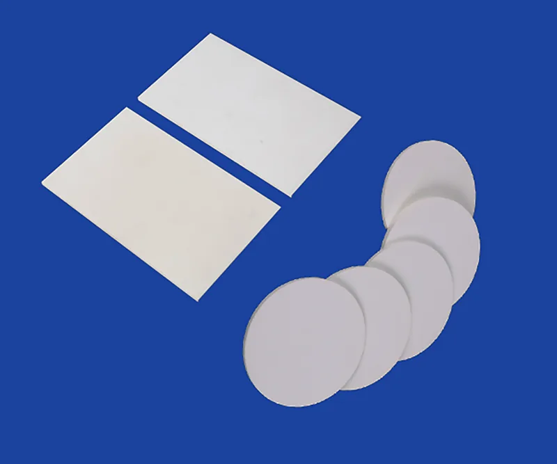
96% and 99.6% Alumina PCB Options
FLJ supplies alumina ceramic circuits in 96% and 99.6% material options. Choose the grade with the conductor process and final surface in mind: a printed hybrid network and a fine deposited pattern ask different things of the same ceramic face.
96% Alumina for Hybrid and Copper Circuits
96% alumina is widely used for thick-film hybrids and selected copper-clad circuits. It provides an insulating carrier for fired conductors, resistors and attached components, or for a bonded copper pattern. Surface condition is matched to the paste or metal-bonding process rather than specified by purity alone.
99.6% Alumina for Thin-Film Circuitry
99.6% alumina is a common choice for fine thin-film patterns and precision sensor circuitry, where a smooth prepared face helps support a continuous deposited layer and defined pattern edges. Specify the required surface state as well as purity; polishing is a separate operation, and the grade name does not establish a finished line-width limit.
Scroll the table horizontally to view all columns.
| Circuit need | Typical grade direction | Surface and route to specify |
|---|---|---|
| Hybrid or thick-film circuit | 96% alumina | Finish matched to the printed conductor process |
| DBC copper construction | 96% alumina is commonly used | Confirm copper-bonding construction and substrate finish |
| Fine sputtered pattern or precision sensor | Consider 99.6% alumina | Define polishing or surface preparation with the thin-film process |
Higher purity is not a universal upgrade for every circuit. The useful specification combines ceramic composition, surface preparation and the conductor system that will be built on it.
Alumina PCB Metallization and Fabrication
FLJ forms plated copper, bonded copper and film circuits on alumina. Each route creates a different conductor-to-ceramic interface, so its pattern geometry, passive elements and component pads are specified as one construction.
DPC Copper Tracks and Component Pads
Direct plated copper (DPC) forms a thin adhesion and seed-metal layer on the ceramic, then builds copper by electroplating. Lithographic patterning defines the tracks and pads. Formed directly on alumina, DPC has no polymer insulation sheet between copper and ceramic. Heat flow still depends on ceramic thickness and the component attachment and cooling path.
After the copper pattern is formed, the background seed metal is removed to electrically separate the tracks. Double-sided designs can also use laser-formed holes and plated walls to connect the two faces; their formation is sequenced with metallization for the selected route. The copper build and pattern are developed together: a thicker conductor needs room at its edges, while the pad finish must suit the selected solder or bond connection.
DBC Copper for Power Circuits
Direct bonded copper (DBC) uses copper foil bonded to the ceramic at high temperature. The foil is then etched into the required pattern. Its broad copper sections carry power and spread heat, while alumina separates conductor regions electrically. DBC suits power circuits where current capacity, thermal path and construction must be considered together.
The copper sheet is etched into separate current paths and connection areas. As copper gets thicker, etching requires wider features and gaps; the capability examples below show this relationship with matched ceramic and copper thicknesses. Fine DPC spacing cannot simply be carried across to a thick DBC power pattern.
Thin initial metallization supports copper growth; exposed background seed is removed to isolate circuits.
A bonded sheet is etched into the power pattern. Copper thickness influences track width and spacing.
Thick-Film and Thin-Film Circuits
Thick-film circuits are made by screen-printing conductive, resistive and dielectric pastes onto alumina and firing them to form functional layers. Resistors can be trimmed after firing, and components can then be attached to create a hybrid circuit. This route integrates passive networks with selected active parts on a compact ceramic carrier; it is different from building copper tracks by DPC plating.
Thin-film circuitry uses deposited metal layers and patterned features, often where a smooth prepared surface and precise geometry are needed. Material grade and final surface preparation are separate choices; composition alone does not define the finished surface. The circuit drawing and assembly method should identify which pads need soldering, wire bonding or another connection, since each requires a compatible metallization system.
Machining, Surface Finish and Circuit Checks
Outline machining, hole formation and metallization are sequenced for the selected route. Mounting holes locate or secure the ceramic; electrical vias need conductive walls and a connection to the circuit pattern. FLJ machines the specified outline and holes, preserves conductor clearance, and finishes the pads for the intended component connection.
Drawing acceptance criteria cover ceramic edge chips or cracks, hole and pad position, and unwanted bridges or interruptions in the metal pattern. Continuity and isolation checks are selected for the required electrical connections. Where interface integrity is part of acceptance, it needs its own agreed inspection or test; an electrical pass alone does not prove metal adhesion.
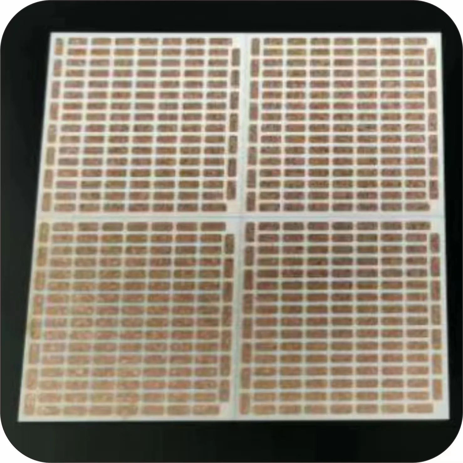
Alumina PCB Specifications and Capabilities
Alumina circuit limits depend on how copper is formed and how thick it is. DPC supports finer traces for compact layouts, while DBC uses thicker bonded copper for broader power paths. The examples below pair each line-and-space figure with its copper construction so the values remain useful for early design selection.
Scroll the table horizontally to view all columns.
| Route | Ceramic construction | Copper | Line / space |
|---|---|---|---|
| DPC | Alumina substrate | 0.5 oz | 3 / 3 mil (about 76 / 76 µm) |
| DPC | Alumina substrate | 1.0 oz | 4 / 4 mil (about 102 / 102 µm) |
| DBC | 0.38 mm ceramic | 0.20 mm per clad side | At least 0.40 / 0.40 mm |
| DBC | 0.63 mm ceramic | 0.30 mm per clad side | At least 0.50 / 0.50 mm |
These are route-specific reference configurations, not one combined set of minimums. The selected alumina grade, surface, outline and panel format are separate design choices; board size, holes and finish should be reviewed against the actual layout. For related process and inspection support, see our manufacturing capabilities.
Applications for Alumina Circuit Boards
Alumina circuits are used as device carriers and functional subcircuits. Their role is specific: connect components, maintain electrical separation and provide a path from the heat source toward the cooling structure.
LED and Optoelectronic Carriers
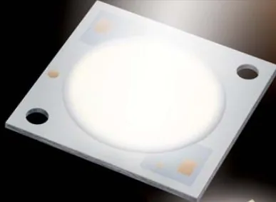
LED emitters and laser packages use defined mounting pads, electrical connections and a route to the cooling surface. A DPC alumina carrier combines the device footprint with plated copper routing. Heat crosses the attachment, copper and ceramic before reaching the external thermal interface; ceramic thickness and the mounting arrangement remain part of that path. Individual carriers or arrays can be supplied to suit package assembly.
Power Switching and Conversion Modules
In inverter and switching modules, broad DBC copper regions connect power devices and carry current while alumina provides electrical insulation. The copper pattern divides the circuit into the required electrical nodes; the ceramic supports these regions above the cooling structure. This is a power-module substrate within the equipment, with conductor spacing and attachment areas chosen for that module.
RF and Precision Hybrid Circuits
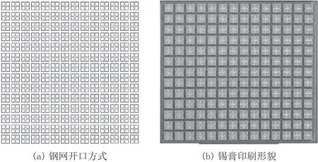
RF attenuators, sensor interfaces and small-signal amplifiers can combine a passive network with attached active devices on alumina. Thick-film conductors and resistors form the network, with laser trimming used to adjust specified resistor values. Thin-film circuitry provides another route for fine deposited patterns on a prepared surface. These are compact functional circuits within an instrument or communications assembly.
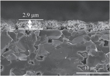
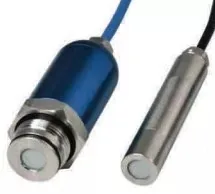
Ceramic also supports functional sensing films. The microscopy reference shows a sensing layer on alumina, while the product photograph illustrates a packaged ceramic-sensor application.
Alumina PCB FAQs
Is an alumina PCB the same as an aluminum-core PCB?
No. Alumina uses aluminum oxide ceramic as its insulating body; an aluminum-core PCB uses a metal core with a dielectric layer. Compare the aluminum-core PCB option for an IMS construction.
How do I choose between 96% and 99.6% alumina?
Start with the circuit and surface. 96% alumina is used for hybrid, thick-film and copper-clad constructions; 99.6% is often selected for smoother surfaces for thin-film patterns. Purity alone does not specify finish or guarantee every property.
When should I choose DPC, DBC or a film circuit?
Choose DPC for patterned plated copper and fine features; choose DBC when bonded, thicker copper supplies the area needed for power. Thick-film uses printed conductors and compatible passive elements; thin-film suits fine deposited patterns on a smooth surface.
Can an alumina board have electrical vias as well as mounting holes?
Yes. DPC can use metallized holes to connect the two circuit faces and separate unplated holes for mounting. Identify each hole’s function, location and finished dimensions in the drawing; feasibility depends on the construction and geometry.
Can the same board support soldering and specified wire-bonding pads?
Yes, if the conductor system and pad finish suit both methods. Wire bonding depends on the specific metallization and bond interface; a gold-colored finish alone does not establish suitability. Specify wire material, joining process and solder requirements.
When is AlN a better choice than alumina?
Consider aluminum nitride when higher ceramic thermal conductivity is a priority and cost and design constraints fit. Compare both families in the ceramic substrate options against your heat path and assembly needs.
What affects the price and lead time of a custom alumina PCB?
Cost and schedule depend on grade, size, conductor route, copper geometry, holes, finish, quantity and assembly scope. Use the contact page to prepare an email enquiry with the drawing and requirements for a project-specific quotation.
OWN-FACTORY CERAMIC CIRCUIT SUPPLY
Alumina PCB Manufacturing and Assembly Services
FLJ manufactures alumina circuits in its own factories, supplying finished bare substrates or populated ceramic assemblies. We match the material and conductor route to the drawing, form the circuit and connection pads, and complete the specified machining and surface finish.
For assembled supply, FLJ combines component sourcing with SMT assembly on the selected ceramic construction. Thick-film hybrids can include printed passive networks and mounted active components; copper carriers can be delivered with the specified component connections. Inspection and electrical checks follow the agreed circuit and assembly requirements.
Assembly inspection addresses the component connections as well as the ceramic circuit, with checks matched to the attachment method and acceptance requirements.
Choose individual circuits or arrays, and bare-board or assembly delivery. For a quotation, include the circuit drawing, grade and surface requirements, ceramic and metal thicknesses, hole and outline dimensions, pad-joining method, quantities and any assembly BOM or acceptance requirements.
Request an Alumina PCB Quote