
IC PACKAGE SUBSTRATE FABRICATION
IC Substrate
PCB Manufacturing
Precision circuitry between the die and the board.
FLJ manufactures BT- and ABF-based package substrates with fine copper circuits, build-up interconnects and connection surfaces for wire-bond and flip-chip packages.
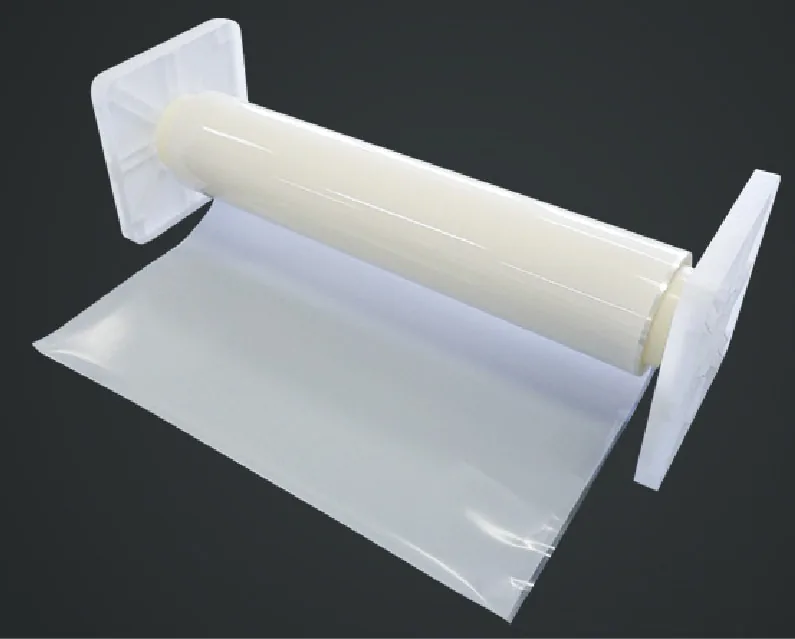
From insulating film to multilayer package circuitry.
IC Substrate Types and Package Interfaces
FLJ manufactures BT- and ABF-based IC package substrates for wire-bond and flip-chip designs, including CSP and BGA package constructions. The substrate carries fine circuitry between the semiconductor die and the contacts that connect its package to a system board. It supplies the routing, power and ground connections, and physical support required by that package.
Wire-Bond and Flip-Chip Substrates
In a wire-bond package, bond fingers on the substrate provide landing points for die-to-substrate wire connections. A flip-chip design instead connects an array of contacts on the die face to corresponding substrate pads. The latter supports dense die-side interconnection in package families such as FC-CSP and FC-BGA, used for devices including processors, ASICs, FPGAs and graphics devices. In either case, the substrate routes those die connections to package contacts that attach the finished package to a board.
BGA identifies a ball-grid-array connection to the board; CSP describes a compact chip-scale package. Wire bonding and flip chip identify the electrical connection from die to substrate. Material and layer construction are further choices, so a flip-chip BGA can use an ABF build-up structure around its selected core.
Single-Die and Multi-Chip Carriers
A single-die carrier fans the chip’s contacts out to the package interface. A multi-chip carrier also routes selected connections between dies, alongside power, ground and board-facing connections. Die placement, routing space and the arrangement of package contacts determine the required circuit layers. These carriers serve processor and logic packages, memory and controller devices, and compact communication or sensor modules according to the selected package design.

Materials and Substrate Construction
Material selection sets the electrical, dimensional and assembly behavior of an IC package substrate. FLJ builds the stack around the package interface, routing density, finished thickness and assembly conditions, choosing core and build-up materials as a coordinated construction rather than as a standalone material specification.
Core and Build-Up Dielectrics
BT, or bismaleimide-triazine resin, is used in package-substrate laminates and prepregs. In a cored organic construction, the selected reinforced laminate provides the central support and its copper circuitry. That core specification is separate from the dielectric used for subsequent build-up layers.
A cored substrate uses a permanent core for structural support, with dielectric and copper build-up layers forming finer routing above and below it. Coreless construction omits that permanent core from the finished stack; it is a distinct stack design, not a synonym for every thin substrate. The choice depends on package design and the required layer arrangement.
For selected build-up designs, ABF is a thermosetting insulating film made from epoxy resin, a curing system and fine inorganic filler. It serves as a dielectric layer, not as a complete substrate. Its surface can be laser processed and metallized with copper to create build-up interconnects. FLJ’s own-factory process integrates the dielectric, laser-formed openings and copper circuit layers into the specified substrate construction.
Thermal and Mechanical Compatibility
Copper patterns, dielectric layers and the core respond differently to temperature changes. Their balance, layer thickness and cure history all influence substrate shape. That makes material and stack design relevant to package assembly: substrate movement during heating can affect alignment and connections even when room-temperature shape appears acceptable.
We balance copper distribution and the layer arrangement around the selected core, and control lamination and curing for that material system. The drawing defines the relevant dimensional and thermal conditions. A finished-substrate thickness is distinct from the thickness of an individual core, dielectric film or plated conductor.
IC Substrate Manufacturing Technology
An IC substrate routes signals laterally between package contacts and vertically between its copper layers. Those paths must meet at small, reliable interfaces: a trace carries a signal across a layer, while a microvia connects that trace to a target pad on another layer. FLJ manufactures package substrates in its own factories, selecting circuit formation and layer construction around the package stack and connection requirements.
Fine-Line Circuit Formation
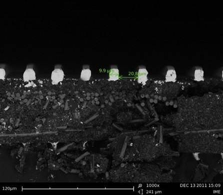
Fine-line circuitry begins with a prepared dielectric surface and a copper-conductor pattern. In a subtractive route, imaging and etching define tracks from a copper layer. Modified semi-additive processing (mSAP) starts with a thin copper layer, plates the imaged circuit pattern, then removes resist and the exposed background copper to electrically separate adjacent tracks. Semi-additive processing (SAP) forms a conductive seed on the dielectric, plates copper where the circuit is required, and removes the resist and exposed seed. FLJ selects the route with the starting material, copper thickness and required circuit geometry.
For these circuits, isolation between neighboring traces matters as much as trace width. Surface preparation must give the copper adequate adhesion while preserving the definition of fine features. If background seed or copper remains between tracks, it can leave an unwanted conductive path; if the dielectric surface is poorly prepared, the copper-to-dielectric interface may not hold as intended.
Build-Up Layers and Microvia Connections
In a build-up stack, an insulating film is laminated over an existing circuit layer. Laser processing opens a microvia through the film to expose its target copper pad. The opening is cleaned and metallized, then copper forms the next circuit layer and the vertical connection into the target. This sequence joins lateral routing on one layer to a defined landing point on the next; the microvia and its target pad therefore form an interface that must be accessible and suitable for copper connection.
Residue at the via bottom can obstruct contact with the target pad. We prepare the exposed copper and dielectric, then control the deposited connection and any specified filling before adding the next layer. Via diameter, land size and registration determine whether the opening reaches the intended copper with the required surrounding margin.
Prepare a thin conductive base on the dielectric.
Build copper in the imaged circuit openings.
Remove resist and exposed background copper.
Package Pads, Surface Finish and Singulation
The finished substrate presents different connection surfaces on the die side and board side. We form the specified pads and solder-mask openings, then apply the finish required for soldering or wire bonding. For ENEPIG-finished connection pads, nickel, palladium and gold are separate layers over prepared copper; layer build, surface condition and the selected wire or solder process determine suitability.
After circuit and surface processing, panels are separated into individual package substrates by singulation. The panel layout, cut paths and edge clearances must preserve the designed contacts and routing. These choices are coordinated with the substrate outline and package interface so the separated part is ready for the next assembly step.
IC Substrate Manufacturing Capabilities
Our IC substrate manufacturing range is organized by package construction. Select the product family first, then match its circuit geometry, dimensions and layer stack to your package.
| Feature | BT FC-BGA | ABF FC-BGA | Wire-bond CSP |
|---|---|---|---|
| Construction / layer count | 1–3 build-up layers per side | 2–6 build-up layers per side | 2, 4, or 6 layers |
| Finished thickness | 0.3–1.2 mm | 0.3–2.4 mm | 0.11–0.56 mm |
| Package dimensions | 8 × 8 to 40 × 40 mm | 8 × 8 to 70 × 70 mm | 3 × 3 to 23 × 23 mm |
| Minimum line / space | 15 / 15 µm | 9 / 12 µm | 30 / 30 µm |
| Blind via / land diameter | 55 / 85 µm | 45 / 75 µm | By design |
| Bond-finger width / space | By design | By design | 90 / 40 µm |
Ranges apply to the indicated product families. The final stack-up sets the central core, copper and dielectric thicknesses, and the combination of feature limits. Surface finish, mask registration and warpage acceptance follow the package drawing and assembly conditions.
Explore our manufacturing capabilities and quality resources for related fabrication, materials and inspection services.
Inspection and Reliability Verification
We inspect the circuit features and interfaces that the package depends on: fine conductors, registered microvias, die-side pads, board-side contacts and the finished substrate shape. Checks follow the selected construction and the acceptance requirements for the supplied substrate.
Circuit and Dimensional Inspection
Optical inspection checks accessible copper patterns for missing features, bridging and registration errors. Dimensional measurements compare line widths, spaces, pad geometry, substrate thickness and outlines with the drawing. Electrical testing checks continuity and isolation against the substrate circuit data, identifying open connections and unintended conductive paths.
The inspection record identifies the measured feature, sample or lot, and applicable specification. Pad pitch, line spacing and finished thickness remain separate measurements; a result for one does not establish the others.
Interconnect and Assembly Reliability
A representative cross-section exposes local via geometry, deposited copper and the interface to its target land. It can reveal details concealed by the finished surface, while electrical testing addresses the network connection. Neither result alone demonstrates the assembled chip’s function or long-term package life.
For builds requiring thermal or environmental qualification, the plan identifies the substrate construction, stress conditions and acceptance criteria. Warpage evaluation states the measurement condition and relevant temperature; room-temperature flatness does not describe all behavior during assembly heating.
Connection-surface checks address the specified metal layers, coverage and handling condition. For a wire-bonded package, the wire material, bonding method and support beneath the pad also enter the joining qualification. These requirements connect substrate delivery to the selected downstream assembly process.
IC Substrate PCB FAQs
How is an IC package substrate different from a standard PCB or SLP?
An IC package substrate routes signals from die-side contacts through dense circuitry to the package connections that meet the board. An SLP is a board-level term; the right construction depends on the package interface and required routing.
Can BT cores and ABF build-up films be used in the same construction?
Yes. A BT core can serve as the base while ABF dielectric layers build up fine interconnects on the surface. They have different roles, so the layer sequence and materials must be specified for the particular substrate design.
How do BGA and CSP packages relate to wire-bond and flip-chip substrates?
BGA describes a ball-grid-array board connection; CSP describes a chip-scale package. Wire bonding and flip chip describe the die-to-substrate electrical connection. For example, an FC-BGA combines flip-chip die connections with a ball-grid-array package interface.
When are subtractive, SAP and mSAP processes used?
Subtractive processing etches tracks from a copper layer. SAP builds the circuit over a deposited conductive seed; mSAP typically begins with thin copper foil. Starting copper, required geometry and the selected stack determine the fabrication route.
What determines the achievable line width, spacing and pad pitch?
These depend on the full design and process combination, including dielectric, copper starting layer, circuit formation, registration and the intended package connections. Line/space and pad pitch are distinct requirements; review them with the layer stack and land pattern.
How is the surface finish selected for flip-chip soldering and wire bonding?
Choose the finish for the electrical joining method and materials. Ni/Pd/Au layers have distinct roles, while wire material, bonding method, surface handling and the supporting stack affect bondability. Gold color by itself does not establish suitability.
How are substrate flatness and warpage addressed for assembly?
Copper, dielectric and core expand differently, so pattern balance, layer thickness and cure history affect shape. Specify the relevant assembly temperature and measurement condition; room-temperature flatness alone does not describe behavior during heating.
What does substrate electrical testing verify, and how does it differ from packaged-IC functional testing?
Bare-substrate electrical testing checks circuit continuity and isolation against the specified network. Packaged-IC functional testing checks the operation of the assembled device, after die connection and packaging. The two tests address different delivered objects.
What affects prototype and production lead times?
Timing depends on the reviewed stack-up, materials, layer count, circuit and via requirements, finish, order quantity and production scheduling. FLJ confirms timing against the actual design and order scope rather than using a fixed delivery promise.
Which drawings and specifications are needed for a quotation?
Provide the layer stack, fabrication data, outline and thickness, via and pad details, finish, tolerances, quantity and any assembly or test requirements. FLJ can review the package details and quote through the contact page.
OWN-FACTORY SUBSTRATE SUPPLY
IC Substrate Fabrication Services and Quotes
FLJ supplies fabricated IC substrates from its own factories, with the defined circuit layers, microvia connections, package pads, surface finish and final outline. Engineering and material support connect the package design to the fabrication route; agreed inspection and release records accompany the supplied build.
For a useful first review, include the package type and wire-bond or flip-chip interface, substrate drawing or stack-up, material and surface-finish requirements, estimated quantity, and target schedule. Add any required inspection criteria if they are already defined. If the design is still in development, send the available requirements and note what remains open; we can use that information to clarify the manufacturing scope and next steps.