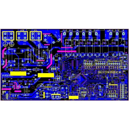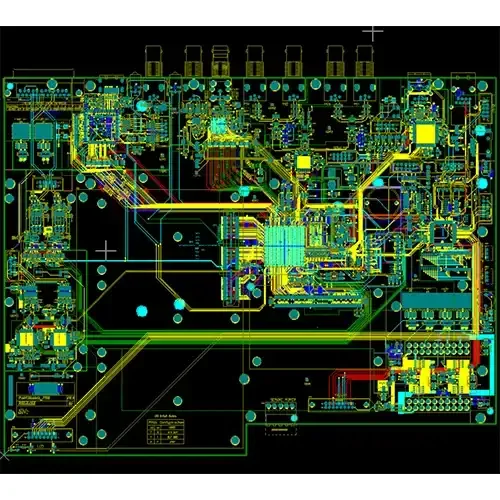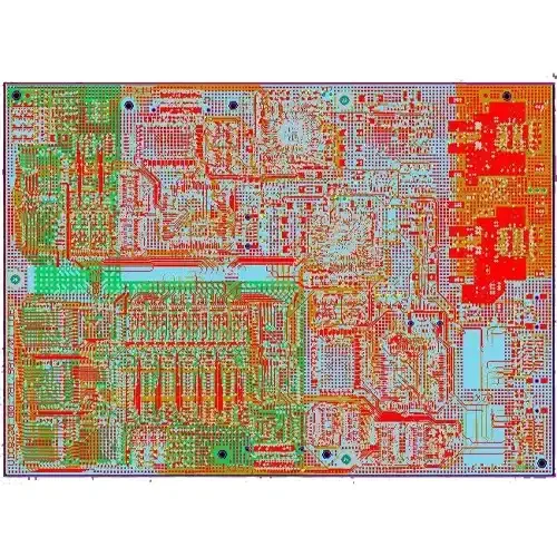
Integrated terminal architecture
- The terminal design combines multiple modules with a dual-system architecture.
- A HiSilicon image-encoding subsystem uses Android.
- A Rockchip image-decoding subsystem uses Linux.
PCB design parameters
| PCB layers | 8 layers |
|---|---|
| Base material | Htg170 |
| Board dimensions | 185*124.5*1.6mm |
| Surface-finish options | Immersion gold |
| Copper weight | 1OZ |
| Minimum line width | 4MIL |
| Minimum spacing | 4MIL |
| Minimum hole diameter | 8MIL |
| Impedance control | +/-10% |
PCB terminal blocks and connections
A PCB terminal block is a modular insulated component mounted on a printed circuit board to secure and connect two or more wires. Its simplest form combines several individual terminals in a strip.
Terminal blocks provide connections for signal, data and power transmission to a PCB. They are used across many industries and in Industry 4.0 applications.
Terminal-block formats include metric and imperial pitches. COMBICON XS-to-XXL terminal-block formats spans miniature 2.5 mm-pitch terminals through to 20 mm-pitch power terminals.