
Bare-die interconnects · PCB & hybrid assemblies
Wire Bonding Services
Connect die pads to the surrounding circuit with a wire-bonded interconnect.
FLJ coordinates wire bonding through specialist partner factories, bringing the selected bonding work together with PCB or carrier supply, related assembly and project delivery.
Request a Wire Bonding QuoteExplore bond geometry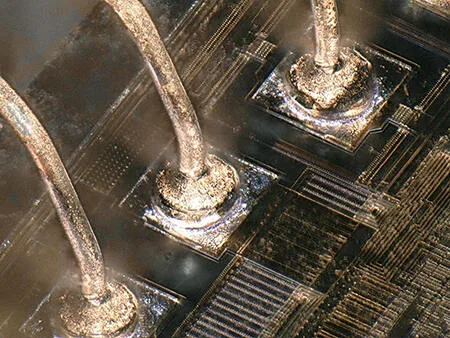
Wire Bonding for PCB and Hybrid Assemblies
A wire-bonded assembly connects a bare semiconductor die to a supporting circuit substrate. Fine wires join pads on the die to matching pads on a PCB, ceramic carrier, or another die. The die attachment holds the chip in position; the bond wires provide the electrical paths between its pads and the surrounding circuit.
One project contact for the die and carrier requirements, related PCB fabrication or assembly, manufacturing changes and delivery. The quotation identifies the supplied operations and required inspection records.
The partner factory performs the selected bonding work. Die attachment, protection and additional testing are included when they form part of the quoted assembly scope.
Chip-on-Board Interconnects
In a chip-on-board (COB) build, one or more bare dies sit directly on a PCB. Their die pads connect by wire to board pads, carrying selected signals or power into the larger circuit. This arrangement can suit compact sensor, optoelectronic, or control modules when the design needs a small bare-die interconnect. The board layout must provide bondable pads around the die and leave room for the wire loops and any later protection or assembly steps.
Ceramic and Hybrid Microelectronic Assemblies
A ceramic carrier can support patterned conductors and a mounted die in a hybrid circuit. Ceramic provides an insulating, mechanically supporting base; its metallized regions form the connection pads, while bond wires make the local die-to-carrier links. Related constructions include component submounts, power substrates, and hybrid circuits. The ceramic shape and metal pattern belong to the carrier design; wire bonding connects the selected die pads to the prepared conductor pattern.
FLJ supplies patterned ceramic carriers and hybrid circuits with the conductors and connection surfaces needed for assembly. The wire-bonded interconnect joins the die to that prepared circuit.
Wire Bonding Methods and Materials
Ball and Wedge Bond Geometry
Bond geometry describes the two contacts and the wire loop between them. A typical forward ball–stitch connection starts with a ball on the die and ends with a flattened stitch on the carrier. Wedge–wedge bonding forms flattened contacts at both ends without first forming a ball.
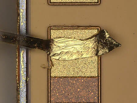
The micrograph shows one flattened contact. The drawings below locate both contacts within the complete connection; tool access and the wire path help determine which form suits the layout.
A stud bump is a local raised contact, rather than a wire spanning two pads. Ribbon describes a flat conductor cross-section. Neither term is a substitute for specifying the complete connection.
| Bond form | First and second contacts | Tool and path considerations | Useful design information |
|---|---|---|---|
| Ball–stitch | A ball first bond and a stitch second bond, joined by the wire loop. | Capillary access at both pads, room to form the loop, and clearance around the die edge. | Die and carrier pad locations, pad sizes, wire specification and permitted loop envelope. |
| Wedge–wedge | A wedge-tool contact at each end, with no initial ball. | Wire feed and tool orientation relative to the connection; access past adjacent or recessed features. | Connection direction, pad geometry, surrounding feature heights and wire or ribbon section. |
Gold, Aluminum and Copper Wires
Gold, aluminum and copper describe the wire material. Gold can be used in ball or wedge processes; aluminum is commonly associated with ultrasonic wedge bonding. Copper is another wire choice requiring a suitable tool, process and pad combination. Material and bond shape are separate decisions.
Thermocompression combines heat and force; ultrasonic bonding combines force and ultrasonic motion; thermosonic bonding also applies heat. These energy routes describe how the contact is formed, rather than the metal used.
Specify wire composition and diameter, or ribbon width and thickness, alongside the die and carrier pad metallurgy. The exposed finish and underlying layers must suit the selected connection. A surface combination qualified for an aluminum-wire application does not establish gold- or copper-wire compatibility. FLJ confirms the proposed material and process combination with the partner factory for the project.
Bond Pads, Loop Design and Assembly Integration
Bondable Surfaces and Stable Support
A reliable wire bond begins with the actual pad stack and its condition, not its color or appearance alone. The bond area needs compatible metallization and a clean surface; residues or oxidation can interfere with intimate contact. Pad layers and the structure beneath them also need to withstand the bonding load. A change to pad metallurgy can therefore affect bondability even when the layout looks unchanged.
The die and carrier need stable support under the bonding tool. With adhesive die attachment, the selected cure and fixation state must support the bonding operation. Movement or flex under load changes contact at the pad and how the applied energy reaches the interface.
Bonding force establishes contact; controlled ultrasonic motion promotes local deformation and joining at the interface during the selected time interval, while applied heat changes the material response. Too little effective energy can leave an incomplete connection. Excessive force or ultrasonic input can damage the pad or underlying structure. Wire, tool, surface and geometry therefore define a process window together.
For PCB carriers, FLJ fabricates ENEPIG-finished pads for specified wire-bonding processes, with the Ni/Pd/Au stack and surface handling matched to the selected connection.
Loop Clearance and the Assembly Sequence
Loop height and span must suit the space around the die and the neighboring wires, components and enclosure. Tool access to both bond locations is part of that geometry. The planned route also has to leave room for subsequent assembly steps, such as nearby soldering, handling or inspection, without creating contact or damage risks for the wire loops.
Nearby soldering and cleaning can alter a reserved bonding surface. Solder reaching a wire-bond pad covers the metal the tool was intended to contact; later operations can also damage exposed loops. The layout and sequence must protect both. FLJ connects partner bonding with the required PCB assembly operations around the actual module construction.
Die-attach material secures the chip at the carrier interface; protective encapsulation surrounds the completed interconnect. Their roles and material requirements differ. Conformal coating and glob-top encapsulation are not interchangeable descriptions of protection. The selected coverage, material and cure belong to the module design.
The relationship below identifies physical roles. The detailed assembly sequence and included protection follow the specified module, rather than a fixed sequence for every product.
- Die attachmentHolds the die on its carrier and provides the support needed for bonding.
- Bonded interconnectJoins the specified pads with two contacts and a shaped wire span.
- Assembly and protectionAccommodates the formed wires, with the included operations and sequence defined for the module.
Wire Bond Inspection and Verification
FLJ coordinates the selected inspection requirements and delivery records with the partner factory. The plan ties each check to a feature, sample and acceptance criterion; the methods below answer different questions about the assembly.
Visual Features and Bond Strength
Visual inspection can assess first- and second-bond placement and visible shape, along with loop profile, heel condition, wire spacing, tail remnants and apparent damage. These observations can flag misplacement, deformation or a visible heel crack; appearance alone does not establish bond strength or electrical function.
Mechanical checks add controlled loading to the visual observations. The force reading needs its test conditions and failure location: a wire, pad or die can fail before the interface being investigated reaches its limit. The table distinguishes those objects.

| Object and method | Question answered | Conditions and results to retain |
|---|---|---|
| Contacts and loop · Visual | Are the intended contacts and wire geometry present, with acceptable visible features? | Inspection scope and criteria; contact placement, loop shape, spacing and visible damage. Appearance does not establish mechanical strength. |
| Wire loop · Pull | How do the wire and its two-ended connection respond to upward hook loading? | Selected hook and loading conditions, force, and break or lift location. The method may pull to break or stop at a specified force; a wire break does not directly measure ultimate bond-interface strength. |
| Bonded metal ball · Shear | How does an applicable ball contact respond to lateral tool loading? | Tool position, support and loading conditions, force, remaining material and pad condition. These help distinguish ball-material failure from interface or pad damage. |
| Die attachment · Die shear | How does the die-to-carrier attachment respond when the die is pushed? | Die, tool and support conditions, force and failure location. Die fracture before interface failure does not establish the attachment interface strength. |
| Specified circuit · Electrical | Does the selected circuit meet its defined electrical or operating requirement? | Circuit and revision, supply or loading conditions, limits and measured response. Electrical success does not replace bond-strength evidence. |
Electrical Checks and Project Records
Electrical and functional checks concern the circuit under its defined operating conditions: continuity of selected connections, isolation or leakage where applicable, or a specified device response. These results complement mechanical evidence. Related board-level electrical and functional verification follows the circuits, supplies, loads and limits selected for the assembled product.
The delivery record should connect the results to the sample or batch, drawing revision, selected method, test conditions and acceptance criteria. FLJ coordinates the required partner records and approved changes through delivery. Sampling, destructive or specified-force tests, and additional electrical coverage are identified for the project.
Request a Wire Bonding Project Quote
Send the die and carrier information needed to define the interconnect:
- Die identification, pad map, connection drawing, pad dimensions and metallization on both sides.
- Required wire material and diameter or ribbon section; loop height, span, clearance and surrounding feature heights.
- Board or substrate drawing, prototype and production quantities, and included die attach, assembly, protection and inspection requirements.
Identify required acceptance criteria and records. FLJ coordinates the project quotation and delivery with the specialist bonding partner.