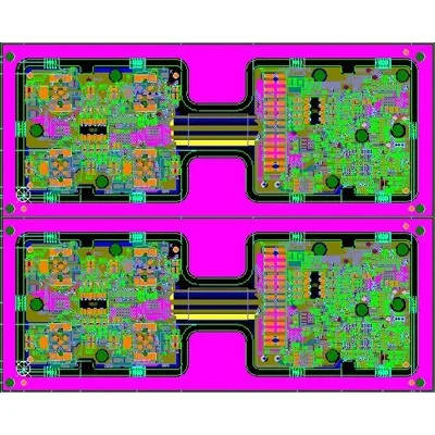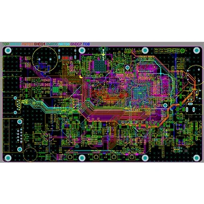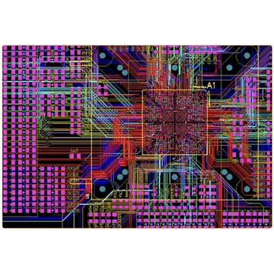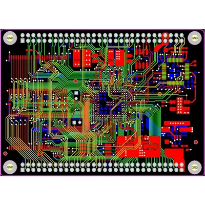
Applications for four-layer HDI designs
Four-layer HDI PCBs are used in telecommunications modules, wireless modules and LED display modules.
- Telecommunications modules
- Wireless modules
- LED display modules
1+N+1 HDI construction
A 1+N+1 construction is the simplest HDI PCB layout structure discussed for BGAs with a relatively low I/O count. Fine conductors, microvias and layer-registration technology support a 0.4 mm ball pitch while maintaining mounting stability and reliable interconnection.
The construction may incorporate copper-filled holes. Materials and surface finishes are selected to support lead-free assembly processes.
Design and manufacturing capabilities
| Capability | Service range or option |
|---|---|
| Material options | IT180, F4BM, FR4, FR1–4 and related materials |
| Design layer range | 1–32 layers |
| Minimum conductor width / spacing | 3 mil |
| Minimum laser-drilled hole | 4 mil |
| Minimum mechanically drilled hole | 8 mil |
| Copper foil thickness | 18–175 µm; standard values: 18, 35 and 70 µm |
| Peel strength | 1.25 N/mm |
| Minimum punched hole, single-sided board | 0.9 mm / 35 mil |
| Minimum hole diameter | 0.25 mm / 10 mil |
| Hole-diameter tolerance for holes ≤0.8 mm | ±0.05 mm |
| Hole-diameter tolerance | ±0.05 mm |
| Hole-wall copper, double-sided / multilayer | ≥0.8 mil |
| Via resistance, double-sided / multilayer | ≤300 µΩ |
| Minimum line width | 0.127 mm / 5 mil |
| Minimum line spacing | 0.127 mm / 5 mil |
| Surface finish options | Rosin flux, HASL, electroplated gold, anti-oxidation treatment, immersion gold and carbon ink |
| Service | OEM service |