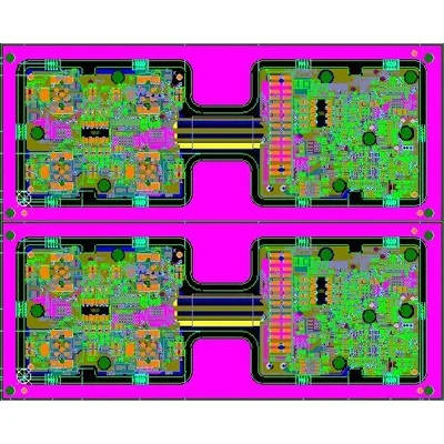
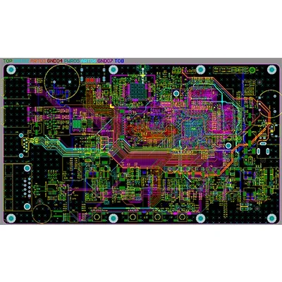
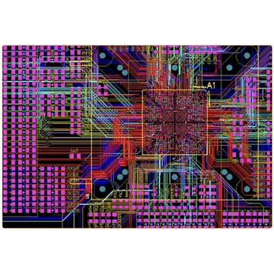
Sixteen-layer routing stackup
A sixteen-layer stack provides sixteen routing layers and is commonly used for high-density designs. When a dense circuit cannot be fully routed within the available layers in an EDA application, additional layers provide further routing capacity.
Sixteen-layer fabrication options
The fabrication discussion covers halogen-free materials, aluminum-based materials, CEM and FR material families.
| Item | Design and fabrication scope |
|---|---|
| Layer count | 16 layers |
| Board thickness range | Up to 7 mm |
| Maximum finished board size | 500 × 500 mm |
| Material families | Halogen-free, aluminum-based, CEM and FR materials |
| Finishing options | Gold plating and silver plating, with halogen-free material options |
Design and manufacturing capabilities
| Capability | Service range or option |
|---|---|
| Material options | TG170 / TG180, F4BM, FR4, FR1–4 and related materials |
| Design layer range | 1–32 layers |
| Minimum conductor width / spacing | 3 mil |
| Minimum laser-drilled hole | 4 mil |
| Minimum mechanically drilled hole | 8 mil |
| Copper foil thickness | 18–175 µm; standard values: 18, 35 and 70 µm |
| Peel strength | 1.25 N/mm |
| Minimum punched hole, single-sided board | 0.9 mm / 35 mil |
| Minimum hole diameter | 0.25 mm / 10 mil |
| Hole-diameter tolerance for holes ≤0.8 mm | ±0.05 mm |
| Hole-diameter tolerance | ±0.05 mm |
| Hole-wall copper, double-sided / multilayer | ≥0.8 mil |
| Via resistance, double-sided / multilayer | ≤300 µΩ |
| Minimum line width | 0.127 mm / 5 mil |
| Minimum line spacing | 0.127 mm / 5 mil |
| Silkscreen colors | Black, white, red, green and other colors |
| Surface finish options | Leaded / lead-free HASL, ENIG, silver and OSP |
| Service | OEM service |
| Standards and compliance references | ISO 9001, RoHS and UL |