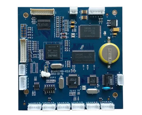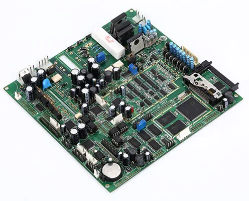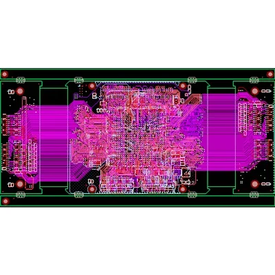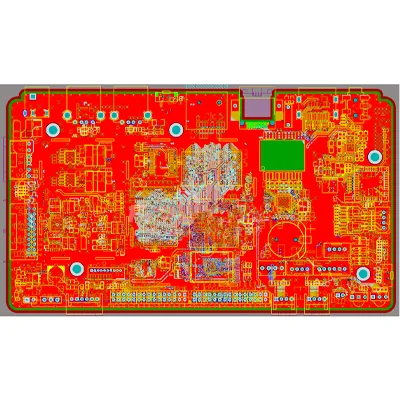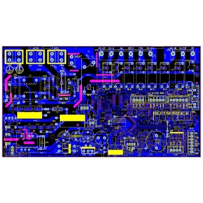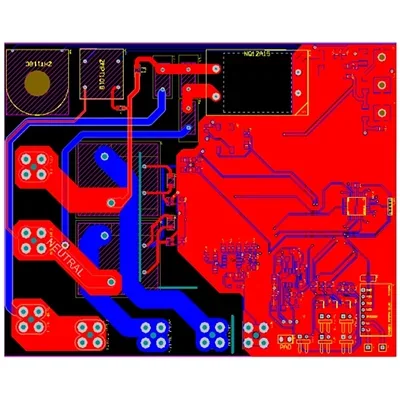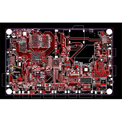
Design and manufacturing capabilities
| Design layer-count capability | 1–32 layers |
|---|---|
| Minimum line width and spacing | 3mil |
| Minimum laser-drilled hole | 4mil |
| Minimum mechanically drilled hole | 8mil |
| Copper foil thickness | 18–175 µm (standard values: 18 µm, 35 µm and 70 µm) |
| Peel strength | 1.25N/mm |
| Minimum punched-hole diameter | Single-sided: 0.9 mm / 35 mil |
| Minimum hole diameter | 0.25mm/10mil |
| Hole-diameter tolerance | For diameter ≤0.8 mm: ±0.05 mm |
| Hole-diameter tolerance | ±0.05mm |
| Plated-hole wall copper thickness | Double-sided / multilayer: ≥0.8 mil |
| Hole resistance | Double-sided / multilayer: ≤300 µΩ |
| Minimum line width | 0.127mm/5mil |
| Minimum spacing | 0.127mm/5mil |
| Legend-colour options | Black, white, red, green and other colours |
| Surface-finish options | Leaded or lead-free HASL, ENIG, silver and OSP |
| Service | OEM services |
| Quality and compliance references | ISO 9001 / RoHS / UL |
Medical RF applications
RF PCBs have been used in medical electronics for many years. X-ray equipment and medical scanners are examples of systems that incorporate RF circuit boards.
The range of medical RF applications also includes implantable medical equipment such as pacemakers.