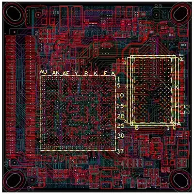
What defines a high-speed board?
High-speed design concerns systems that transfer data between components using high-speed digital signals. The boundary between a high-speed digital design and a simpler board using slower digital protocols is not precise. A commonly used indicator is the edge rate, or rise time, of the digital signals.
Many digital designs combine fast-edge-rate protocols with slower-edge-rate protocols. With embedded computing and the Internet of Things, many high-speed boards also include RF front ends for wireless communications and networking.
Allocating signal, power and ground layers
A high-speed stackup allocates layers to signals, power and ground. Layer planning considers the following factors.
- Board size and net count: Consider the physical board dimensions and how many nets need to be routed. A larger board can provide enough routing space without requiring as many signal layers.
- Routing density: A large net count within a small board area can leave insufficient room for surface routing. More internal signal layers may be needed as conductors move closer together. Reducing the board outline can therefore force a higher routing density.
- Number of interfaces: Depending on bus width, serial or parallel signaling and board size, routing only one or two interfaces on each layer can be an effective approach. Keeping all signals from a high-speed digital interface on the same layer supports consistent impedance and skew.
- Low-speed and RF signals: Determine whether the design also carries low-speed digital or RF signals. These can occupy surface area otherwise available to high-speed buses or components, making additional internal layers necessary.
- Power integrity: Large ICs can require multiple supply voltages. Providing substantial power and ground planes for each voltage is a foundation of power integrity. Adjacent power and ground layers increase plane capacitance and work with decoupling capacitors to support a stable supply.
Design and manufacturing capabilities
| Capability | Service range or option |
|---|---|
| Material options | TG170 / TG180, F4BM, FR4, FR1–4 and related materials |
| Design layer range | 1–32 layers |
| Minimum conductor width / spacing | 3 mil |
| Minimum laser-drilled hole | 4 mil |
| Minimum mechanically drilled hole | 8 mil |
| Copper foil thickness | 18–175 µm; standard values: 18, 35 and 70 µm |
| Peel strength | 1.25 N/mm |
| Minimum punched hole, single-sided board | 0.9 mm / 35 mil |
| Minimum hole diameter | 0.25 mm / 10 mil |
| Hole-diameter tolerance for holes ≤0.8 mm | ±0.05 mm |
| Hole-diameter tolerance | ±0.05 mm |
| Hole-wall copper, double-sided / multilayer | ≥0.8 mil |
| Via resistance, double-sided / multilayer | ≤300 µΩ |
| Minimum line width | 0.127 mm / 5 mil |
| Minimum line spacing | 0.127 mm / 5 mil |
| Silkscreen colors | Black, white, red, green and other colors |
| Surface finish options | Leaded / lead-free HASL, ENIG, silver and OSP |
| Service | OEM service |
| Standards and compliance references | ISO 9001, RoHS and UL |