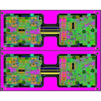
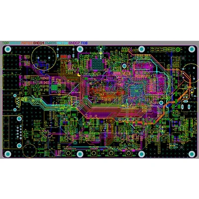
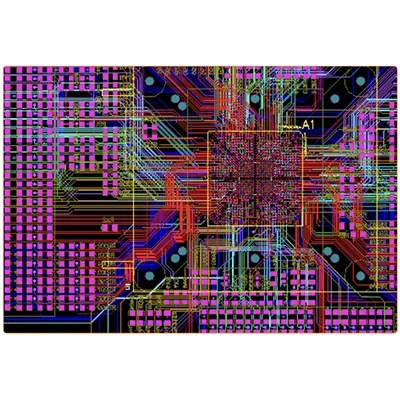
Any-layer HDI interconnection
Any-layer HDI is the most complex HDI construction discussed here. All layers are high-density interconnection layers, allowing conductors on the PCB layers to interconnect through copper-filled stacked microvias.
This structure supports highly complex devices with large pin counts, including CPU and GPU chips used in handheld and mobile equipment. It provides a dense interconnection solution while supporting the electrical requirements of these devices.
Design and manufacturing capabilities
| Capability | Service range or option |
|---|---|
| Material options | TG170 / TG180, F4BM, FR4, FR1–4 and related materials |
| Design layer range | 1–32 layers |
| Minimum conductor width / spacing | 3 mil |
| Minimum laser-drilled hole | 4 mil |
| Minimum mechanically drilled hole | 8 mil |
| Copper foil thickness | 18–175 µm; standard values: 18, 35 and 70 µm |
| Peel strength | 1.25 N/mm |
| Minimum punched hole, single-sided board | 0.9 mm / 35 mil |
| Minimum hole diameter | 0.25 mm / 10 mil |
| Hole-diameter tolerance for holes ≤0.8 mm | ±0.05 mm |
| Hole-diameter tolerance | ±0.05 mm |
| Hole-wall copper, double-sided / multilayer | ≥0.8 mil |
| Via resistance, double-sided / multilayer | ≤300 µΩ |
| Minimum line width | 0.127 mm / 5 mil |
| Minimum line spacing | 0.127 mm / 5 mil |
| Silkscreen colors | Black, white, red, green and other colors |
| Surface finish options | Leaded / lead-free HASL, ENIG, silver and OSP |
| Service | OEM service |
| Standards and compliance references | ISO 9001, RoHS and UL |