RF PCB design and the radio-frequency front end
In a wireless communication system, only a relatively small front-end section operates at radio frequency. The rest of the circuit performs low-frequency baseband analog and digital signal processing. An RF front end commonly includes a low-noise amplifier, a mixer and a power amplifier.
Although the RF front end contains fewer components than the baseband circuitry, it remains central to overall system performance.
The six RF design tradeoffs
RF PCB design processes analog signals across a wide dynamic range at high frequency. Like the multi-parameter tradeoffs often illustrated by an octagonal rule in analog IC design, RF design has its own six-sided balance:
- Noise
- Linearity
- Supply voltage
- Gain
- Operating frequency
- Power
Two or more of these parameters often constrain one another, creating a multidimensional optimization problem. The resulting compromises make the RF designer’s judgment and practical experience important when selecting an appropriate balance.
RF PCB applications
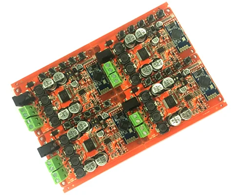
- Base-station RF circuit boards
- Mobile-phone RF circuit boards
- Wireless local-area-network (WLAN) RF PCBs
- Global positioning system (GPS) RF PCBs
- Radio-frequency identification (RFID) boards
- Internet of Things (IoT) RF PCBs
Design and manufacturing capabilities
| Capability | Service range or option |
|---|---|
| Design layer range | 1–32 layers |
| Minimum conductor width / spacing | 3 mil |
| Minimum laser-drilled hole | 4 mil |
| Minimum mechanically drilled hole | 8 mil |
| Copper foil thickness | 18–175 µm; standard values: 18, 35 and 70 µm |
| Peel strength | 1.25 N/mm |
| Minimum punched hole, single-sided board | 0.9 mm / 35 mil |
| Minimum hole diameter | 0.25 mm / 10 mil |
| Hole-diameter tolerance for holes ≤0.8 mm | ±0.05 mm |
| Hole-diameter tolerance | ±0.05 mm |
| Hole-wall copper, double-sided / multilayer | ≥0.8 mil |
| Via resistance, double-sided / multilayer | ≤300 µΩ |
| Minimum line width | 0.127 mm / 5 mil |
| Minimum line spacing | 0.127 mm / 5 mil |
| Silkscreen colors | Black, white, red, green and other colors |
| Surface finish options | Leaded / lead-free HASL, ENIG, silver and OSP |
| Service | OEM service |
| Standards and compliance references | ISO 9001, RoHS and UL |