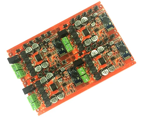
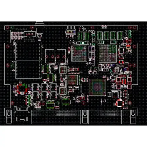
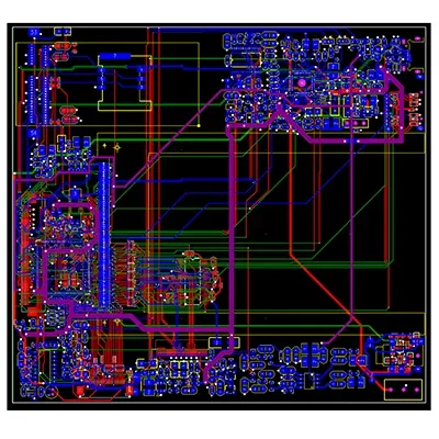
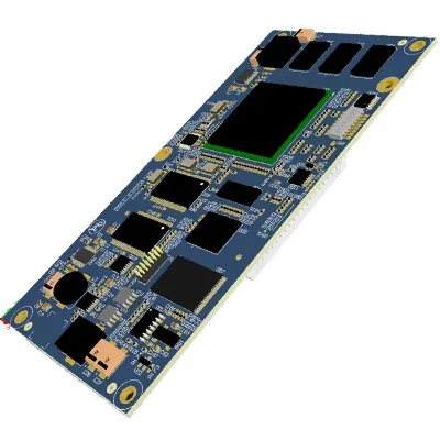
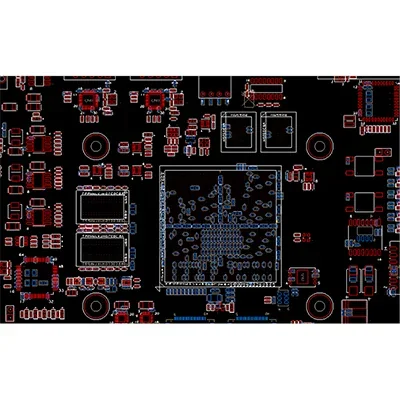
GPS receiver PCB assembly
- Provide the PCB fabrication files and parts list for the project.
- PCB fabrication and circuit-board component procurement are included in the manufacturing scope.
- Populate the PCB with the specified components.
- Perform electronic testing of the circuit board or assembled PCBA.
- Support prompt delivery with anti-static packaging.
- RoHS-compliant, lead-free assembly.
- One-stop support for PCB design, PCB layout, PCB fabrication, component purchasing, PCB assembly, testing, packaging and delivery.
PCBA manufacturing services
- PCB fabrication from 1 to 32 layers, including single-sided, double-sided and multilayer boards, HDI boards, and buried- and blind-via constructions.
- Material procurement and management.
- Quick-turn PCBA prototypes and new product introduction (NPI).
- Surface-mount and through-hole PCB assembly.
- IC pre-programming, functional verification and burn-in testing.
- Complete-unit and box-build assembly, including plastic parts, displays, metal enclosures, membranes, coils and wire harnesses.
- Low-volume production and high-mix model solutions.
- Automated optical inspection (AOI), in-circuit testing and BGA placement.
- Engineering support for end-of-life and obsolete-component replacement, together with design support for circuits, metal parts, plastic enclosures and packaging.
PCB manufacturing capabilities
| Manufacturing parameter | Capability |
|---|---|
| Surface finishes | HASL; electroplated gold; immersion gold; gold-finger plating; OSP; flux |
| Layer range | 1–32 layers |
| Copper thickness | 0.5–5 oz |
| Board thickness | 0.2–6.0 mm |
| Minimum hole size | 0.2 mm |
| Minimum line width | 0.1 mm |
| Minimum line spacing | 0.1 mm |
| Maximum board size | 508 × 609 mm |
| Solder mask colors | Green, black, red, yellow, white and blue |
| Silkscreen colors | White, yellow and black |
| Manufacturing data | Gerber files with corresponding drill files; PROTEL-series data; bill of materials |
| Base materials | FR4, CEM3, PTFE, aluminum-based materials, high-Tg FR4, high-frequency laminates and Rogers materials |
PCBA manufacturing lead time
Sample delivery is 10–15 days after the OEM agreement is signed and the engineering documents are confirmed.
Mass-production delivery can be arranged in several batches according to customer requirements.