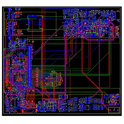
Design and manufacturing capabilities
| Base-material options | IT180, F4BM, FR4, FR1-4 and related materials |
|---|---|
| Design layer-count capability | 1–32 layers |
| Minimum line width and spacing | 3mil |
| Minimum laser-drilled hole | 4mil |
| Minimum mechanically drilled hole | 8mil |
| Copper foil thickness | 18–175 µm (standard values: 18 µm, 35 µm and 70 µm) |
| Peel strength | 1.25N/mm |
| Minimum punched-hole diameter | Single-sided: 0.9 mm / 35 mil |
| Minimum hole diameter | 0.25mm/10mil |
| Hole-diameter tolerance | For diameter ≤0.8 mm: ±0.05 mm |
| Hole-diameter tolerance | ±0.05mm |
| Plated-hole wall copper thickness | Double-sided / multilayer: ≥0.8 mil |
| Hole resistance | Double-sided / multilayer: ≤300 µΩ |
| Minimum line width | 0.127mm/5mil |
| Minimum spacing | 0.127mm/5mil |
| Surface-finish options | Rosin flux, HASL, electroplated gold, anti-oxidation treatment, immersion gold and carbon ink |
| Service | OEM services |
Communications applications
Communications PCBs are used in general telecommunications systems, including mobile-phone towers, satellites, high-speed routers, servers and business telephones. Telecommunications PCBs are also used to control LED displays and indicators.
Hybrid high-frequency board construction
A hybrid high-frequency board combines a base with inner and outer circuit layers and solder-mask layers. Its substrate is divided into a high-frequency area and an auxiliary area. The auxiliary area provides mechanical support, while the high-frequency inlay is held in its designated position.
Separating the high-frequency area allows high-frequency material to be used only where it is needed. This arrangement meets the high-frequency signal requirements while reducing the quantity of high-frequency laminate used and controlling production cost.