Design and manufacturing capabilities
| Base-material options | IT180, F4BM, FR4, FR1-4 and related materials |
|---|---|
| Design layer-count capability | 1–32 layers |
| Minimum line width and spacing | 3mil |
| Minimum laser-drilled hole | 4mil |
| Minimum mechanically drilled hole | 8mil |
| Copper foil thickness | 18–175 µm (standard values: 18 µm, 35 µm and 70 µm) |
| Peel strength | 1.25N/mm |
| Minimum punched-hole diameter | Single-sided: 0.9 mm / 35 mil |
| Minimum hole diameter | 0.25mm/10mil |
| Hole-diameter tolerance | For diameter ≤0.8 mm: ±0.05 mm |
| Hole-diameter tolerance | ±0.05mm |
| Plated-hole wall copper thickness | Double-sided / multilayer: ≥0.8 mil |
| Hole resistance | Double-sided / multilayer: ≤300 µΩ |
| Minimum line width | 0.127mm/5mil |
| Minimum spacing | 0.127mm/5mil |
| Surface-finish options | Rosin flux, HASL, electroplated gold, anti-oxidation treatment, immersion gold and carbon ink |
| Service | OEM services |
How a four-layer PCB is arranged
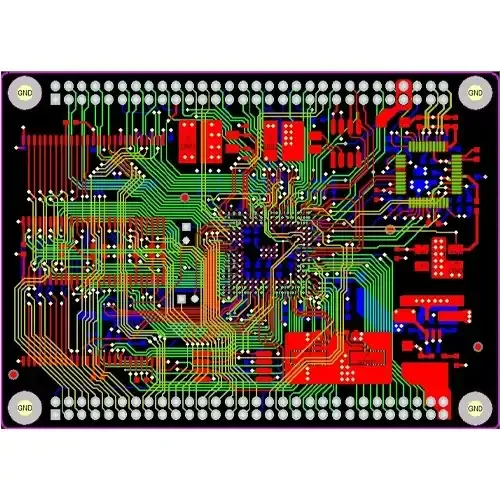
A four-layer PCB has four conductive layers for routing electrical signals: the top layer, inner layer 1, inner layer 2 and the bottom layer. The top and bottom layers are the outside layers used for component placement and routing.
The two inner layers are located within the board and are commonly used as power planes or signal-routing layers. Possible arrangements include three signal layers plus a ground layer, or two signal layers plus a VCC power layer and a ground layer.