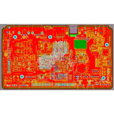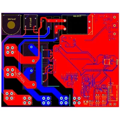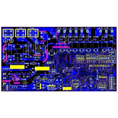
PCBs in medical electronics
Printed circuit boards have expanded across many areas of electronics, including IoT equipment, smartphones, computers and artificial intelligence. Their role in medical equipment connects electronic development with the needs of patients and healthcare professionals.
PCBs make compact medical devices possible. Improvements in healthcare technology help address tasks such as accurate diagnosis and monitoring a patient’s health condition.
A forecast for 2022 projected the global medical-electronics market at US$4.4 billion. The growth discussed in that forecast reflects the increasing role of PCBs as medical equipment becomes digital and depends on electronic functions for efficient operation.
Examples include defibrillators, electrical muscle-stimulation equipment, MRI systems, medical imaging systems, CT scanners and ultrasound equipment.
Reliability, cleanliness and compact construction
Medical PCB production requires particular care because the reliability of the equipment can affect a person’s life. Cleanliness requirements are especially demanding for circuitry intended for implantable equipment.
These designs must be clean and compact. High-density interconnect (HDI) technology supports the small dimensions and dense component placement needed by many medical devices.
HDI and via-in-pad technology
Via-in-pad places a via inside a copper pad to conserve PCB area. The design discussion describes making as much as 50% of the available area accessible for component placement, helping engineers achieve suitable pitches in smaller equipment.
Blind and buried vias also reduce routing space and increase component density. Via-in-pad is an important option where high-speed interconnection and high dissipation must be addressed in a dense board layout.
Surface-mount technology
Surface-mount technology (SMT) is widely used in commercially manufactured electronic equipment. Smaller SMT components allow more electronics to fit into a compact space.
SMT also supports automated soldering and PCB assembly, improving manufacturing repeatability and reliability while helping control assembly cost.
Fine conductors and spacing
The next generation of portable electronics relies on HDI constructions with very fine lines and spaces. Compared with conventional routing technology, fine-feature HDI can reduce board dimensions, improve routing density and help control manufacturing cost.
Medical industry applications
PCBs and electronics support medical appliances as well as monitoring, diagnostic and treatment equipment. As the technology develops, their use across healthcare continues to expand.
- Scanning equipment: CT scanners, X-ray displays and ultrasound scanners depend on electronic components.
- Patient monitoring: Heart-rate, blood-glucose and blood-pressure monitors all incorporate electronic circuitry.
- Medical and research instruments: Data collection and testing equipment includes electron microscopes, control systems, compressors and other instruments using PCBs.
Design priorities for medical equipment
Healthcare applications place high demands on reliability and quality. At the same time, the dimensions of the host equipment restrict the PCB outline. Medical PCB development therefore combines dependable construction with continuing miniaturization.
Design and manufacturing capabilities
| Capability | Service range or option |
|---|---|
| Material options | IT180, F4BM, FR4, FR1–4 and related materials |
| Design layer range | 1–32 layers |
| Minimum conductor width / spacing | 3 mil |
| Minimum laser-drilled hole | 4 mil |
| Minimum mechanically drilled hole | 8 mil |
| Copper foil thickness | 18–175 µm; standard values: 18, 35 and 70 µm |
| Peel strength | 1.25 N/mm |
| Minimum punched hole, single-sided board | 0.9 mm / 35 mil |
| Minimum hole diameter | 0.25 mm / 10 mil |
| Hole-diameter tolerance for holes ≤0.8 mm | ±0.05 mm |
| Hole-diameter tolerance | ±0.05 mm |
| Hole-wall copper, double-sided / multilayer | ≥0.8 mil |
| Via resistance, double-sided / multilayer | ≤300 µΩ |
| Minimum line width | 0.127 mm / 5 mil |
| Minimum line spacing | 0.127 mm / 5 mil |
| Surface finish options | Rosin flux, HASL, electroplated gold, anti-oxidation treatment, immersion gold and carbon ink |
| Service | OEM service |