
















PCB Panelization for SMT Assembly: A Practical Design Guide
A good SMT panel gives the assembly line a stable board to transport, an accurate reference to locate, and a controlled way to separate the finished PCBAs. Start with those three jobs before deciding how many boards to squeeze into the array.
The layout with the most boards isn’t always the cheapest to build. It may block a conveyor, leave a board unsupported during printing, or put a ceramic capacitor next to a cut that flexes the assembly. Those problems show up after the bare-board layout looks finished.
This guide walks through the decisions that matter: the handling envelope, registration features, separation method, component risks, and release package. You’ll also see a design example and a way to compare panel costs without confusing board count with production throughput.
Jump to: Rails and support · Fiducials · V-score vs. routing · Component risks · Release files
First, decide what the panel has to do
Fabrication and assembly need different approvals
A fabrication panel groups circuits for bare-board processing. An assembly panel carries the circuits through solder paste printing, placement, reflow, inspection, and sometimes testing. The fabricator may produce several assembly arrays within a larger manufacturing panel.
That distinction changes the drawing you need to approve. A layout that uses laminate efficiently can still be awkward for SMT assembly. The fabrication review covers features such as routing and scoring. The assembly review covers gripping, support, registration, populated clearances, and separation.
Use one-up, multi-up, or a carrier for a reason
A small or irregular PCB often needs an array to become a practical handling unit. A larger board may need only a single-up frame with rails. A reusable carrier may be worth discussing when a thin board or unusual outline can’t support itself through the intended process.
Mixed-design panels need an extra check: demand. If every panel produces three boards of design A and one of design B, your replenishment orders inherit that ratio. A revised or discontinued design can make the shared array expensive to maintain. Use mixed arrays when the production requirements support them.
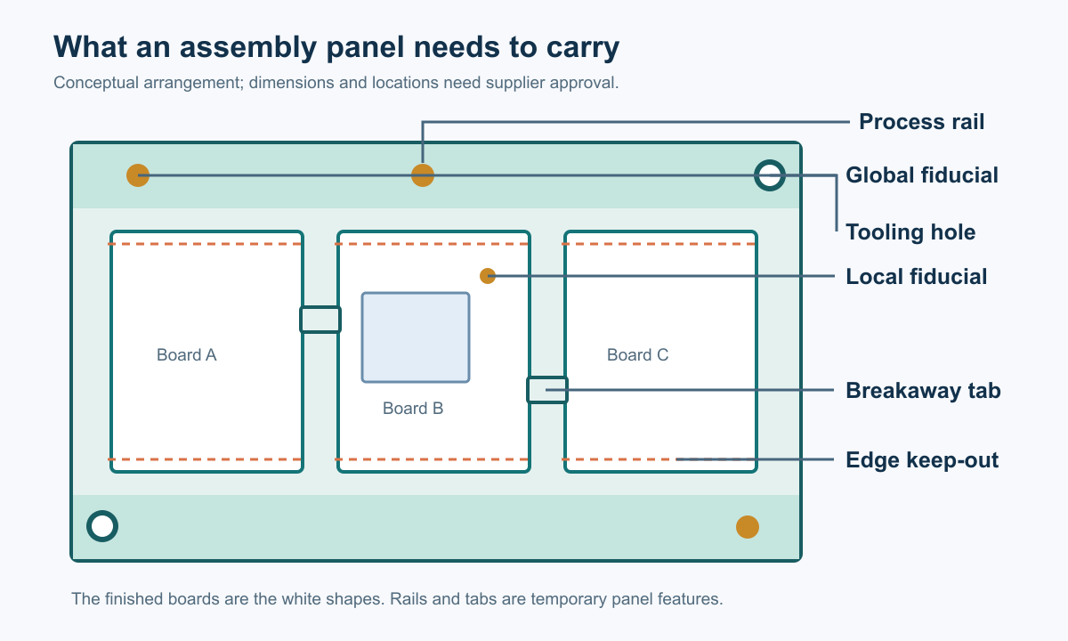
Illustration: The frame provides handling and registration features around the individual boards. This is a schematic, not a dimensioned production drawing.
Rails and support: plan for the populated board
Check the full handling envelope
Start with the finished assembly in 3D, including both sides. A connector can extend beyond the PCB outline. A tall capacitor can interfere with a clamp. An underside component can occupy the space a support pin needs.
Show these features on the panel drawing:
- The proposed conveyor edges and feed direction.
- Top and bottom component height envelopes.
- Parts that overhang the board edge.
- Areas where clamps, supports, and cutting fixtures may contact the panel.
Rail width alone doesn’t settle these questions. The relevant clearance is between the equipment and the populated assembly throughout its route.
Keep the printer from pushing an unsupported board
During printing, the board must stay supported against the stencil. Long routed openings, narrow connecting webs, or a large central span can make an array too flexible for the support arrangement.
For a double-sided build, review the second print separately. Components already soldered to the first side may sit beneath the panel. The support setup must avoid them while still holding the next print surface stable. A support conflict can require a different tab pattern, a smaller array, or dedicated tooling.
When reviewing SPI measurements, keep panel support on the troubleshooting list. An apparent print problem may involve the board’s mechanical setup as well as paste or stencil settings.
Don’t let one machine define the whole panel
Check the panel against every planned operation, including inspection, test fixtures, and depaneling. A placement machine’s working area doesn’t establish the limits of the downstream equipment.
Also ask how the array behaves when heated and moved. A heavy connector at one end or an unevenly supported board can change the handling problem after reflow. Put the actual material, thickness, and component distribution in the review package. A generic rail dimension can’t account for all three.
Fiducials and tooling holes: give each feature a job
Fiducials locate copper; holes locate fixtures
Fiducials are optical reference marks. Tooling holes provide mechanical location or restraint for a particular fixture. They serve different purposes, so adding one doesn’t automatically remove the need for the other.
Specify the fiducial copper feature, solder mask opening, and surrounding clear area together. Keep the mark visible to the camera and clear of clamping hardware. Panel fiducials establish the array reference; board or local fiducials may be needed for the placement strategy.
Tooling holes need their own diameter, location, tolerance, and plating instruction. Use the fixture owner’s requirements.
Make orientation obvious in the data and on the panel
A symmetric array can look correct when loaded backward. Use a clear orientation convention and identify the feed direction. The registration pattern and visible markings should help an operator recognize the intended orientation.
Keep the CAD array, placement files, and inspection mapping consistent. Rotating alternate boards may improve nesting, but the programming must include those rotations. Confirm whether the assembler wants individual-board placement data plus an array map or a fully panelized placement file. Supplying both without identifying the controlling file creates avoidable ambiguity.
V-score or tab routing? Choose the cut before the array
V-scoring suits continuous straight boundaries
V-scoring leaves a reduced section of laminate along a straight separation line. It can be useful for rectangular boards with shared edges.
The remaining material must keep the panel stable through assembly while allowing the intended separation process. A drawing that says only "V-score" leaves that balance unresolved. Agree on the score geometry, finished thickness, and separation equipment with the manufacturing team.
Check access above and below the score line too. Components may obstruct the separator even when the bare-board geometry is suitable. A scored panel should have a defined separation operation; "snap it apart" isn’t a complete production instruction.
Routed tabs give you more control over the outline
Tab routing removes material around the board while leaving bridges to retain it. This gives more freedom to place the retaining features around irregular outlines.
Tab placement affects panel stiffness, cutting access, and the finished edge. Perforated mouse-bite tabs still leave material to break or remove. If a tab sits on an enclosure datum, card-edge interface, or visible product edge, specify how the remnant will be finished and inspected.
Don’t choose the tab pattern from a screenshot. The board thickness, span, assembly weight, and cutting fixture determine whether the proposed bridges are appropriate.
Compare the methods against the actual assembly
| Decision | V-score | Routed outline with tabs |
|---|---|---|
| Starting geometry | Continuous straight boundaries | Shaped outlines and selective retaining locations |
| What needs review | Remaining web, separator access, bending during separation | Tab positions, tool access, support and remnant finishing |
| Edge-sensitive parts | Review clearance and strain along the score | Place and cut tabs around protected component zones |
| Finished edge | Specify the required profile after separation | Identify where tab remnants are acceptable |
| Typical tradeoff | Compact spacing with constrained cut geometry | More layout freedom with routing space and tooling needs |
Other methods, including laser separation, may be worth evaluating for suitable materials and assemblies. Availability, edge condition, cleanliness, thermal effects, and cost need a specific process review. Treat the cutting method as part of the build definition.
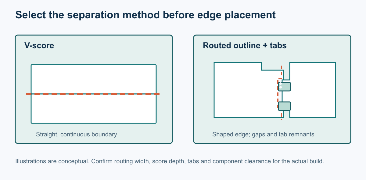
Illustration: The cut geometry determines where boards can sit and where they remain attached. The diagram does not specify score depth, routing width, or production clearances.
Protect components from the separation process
Review strain at ceramic components
Board bending can transfer stress into soldered components. Ceramic capacitors deserve particular attention near separation features. Murata’s capacitor layout guidance explains how placement and orientation near board breaks affect stress.
Use that guidance to review the actual component layout with the design owner. Moving a tab, changing support near the cut, or selecting a different separation process may help. Simply rotating a component doesn’t establish that the finished assembly is safe.
For a sensitive design, ask what evidence will qualify the separation process. Depending on the product, that may include instrumented strain measurements and checks beyond a visual inspection.
Include connectors, BGAs, and underside parts
Mark components whose bodies, joints, or mounting features could be affected by bending or cutting. A connector overhang may block tool access. A large package may limit where the board can be held. A bottom-side part can collide with a support that looks harmless in the top view.
Review the cutting tool’s working envelope, the fixture, and the part placement together. A component keepout drawn only from the nominal PCB edge misses these interactions.
Define edge quality and cleanliness
State which finished edges locate the PCB in its enclosure and which can tolerate a residual tab. Include burr, debris, and cosmetic requirements where they affect the product.
Cutting and cleanup also need a place in the process sequence. If a sensitive connector or an already-coated assembly is present, discuss how the selected method will control debris and protect surfaces. A clean-looking edge doesn’t prove that the handling or separation step was harmless to the components.
A design example: the panel that fits but won’t release cleanly
The first proposal
Consider an illustrative rectangular control board with an edge connector on one side and a ceramic capacitor near the opposite edge. The proposed array uses shared V-score boundaries and packs the boards tightly.
The bare-board drawing appears efficient. The populated review reveals two questions: can the separator pass the connector, and how will the board be supported while the opposite edge is separated?
Increasing the rail width won’t necessarily solve either problem. The difficult features are at the product boundary.
The revised proposal
A routed array could place tabs on less sensitive edges and reserve fixture contact areas away from components. The connector edge could remain free of tab remnants. The capacitor region would still need review for the actual cut and support sequence.
The revised drawing should identify protected component zones, approved contact areas, cut order, and final edge requirements. Compare that proposal with a revised scored layout before choosing.
This is a design scenario, not a reported FLJPCB production result. Its purpose is to show how the decision changes once you review the assembly instead of the empty outline.
Inspection, test, and bad board positions
Keep each board’s identity after the rails are gone
Give repeated circuits clear position identifiers. Inspection and test records should identify the panel and the board position when the array is still intact.
Decide when the individual assembly gets its permanent identity. A barcode on a removable rail won’t identify the board after separation. If you rely on tray positions during the transition, define how that mapping is maintained.
The PCBA test-plan guide covers test evidence in more detail. For panel design, the key question is whether access and identification survive the planned sequence.
Agree on how rejected positions are handled
A fabricated array may contain a rejected circuit position, often described as an X-out. Whether those arrays are allowed is an order requirement.
If they are allowed, agree on identification, programming, paste printing, component placement, and test handling for the rejected position. Confirm whether a modified stencil or another approved method is needed. Don’t assume one mark automatically tells every machine to skip the same circuit.
This decision also affects purchasing quantities. The number of usable positions can differ from the nominal number of cavities.
What panelization really changes about cost
Board count isn’t a throughput multiplier
An array can spread handling and some setup work across several boards. Placement time still depends on the components to be placed, and inspection or testing may require work at every position.
A larger array can also bring more demanding support, tooling, or separation requirements. Ask for a comparison that includes fabrication, stencil, assembly, inspection, test, depaneling, edge finishing, and packaging.
Compare the same number of accepted PCBAs
Here’s simple planning arithmetic, not a supplier quote: an order for 500 accepted boards needs at least 125 four-up panels or 63 eight-up panels, assuming every position is usable. The eight-up option provides 504 positions.
Those counts are only a starting point. Any allowance for rejected positions, setup loss, or assembly rejects changes the order plan. Compare quotes using the same accepted delivery quantity and the same inspection and test scope.
For mixed designs, include excess inventory from the fixed panel ratio. A lower fabrication cost can lose its advantage if you repeatedly build boards you don’t need.
What to send with your panelization request
Send data that lets someone check the proposed array
Use the broader PCB quotation checklist for the order package. Add these panel-specific details:
- Released PCB outline, material, stackup, and finished thickness.
- Assembly data for both sides, including overhangs and height information.
- Proposed array drawing, board count, orientation, and position map.
- Rails, fiducials, tooling holes, score lines, or tab locations.
- Protected component zones and permissible fixture contact areas.
- Separation, finished-edge, cleanliness, test, and traceability requirements.
- Required delivery form: assembled panels or separated PCBAs.
Freeze the panel revision before tooling and programming
Give the panel drawing its own revision and tie it to the PCB and assembly revisions. A change in array pitch, board rotation, or fiducial location can affect the stencil, placement program, inspection map, and fixture.
Require a change review after release. "Same PCB, different panel" may still mean different production files and tooling. Identify which version applies to each build.
Ask for three concrete outputs
For a FLJPCB PCB assembly review, request an approved array drawing, a handling and support plan, and a defined separation method.
If a feature doesn’t work, ask the reviewer to mark the conflict and propose the change: move a tab, create tool clearance, reduce the array, or provide a fixture. That gives your design team something specific to act on before production starts.