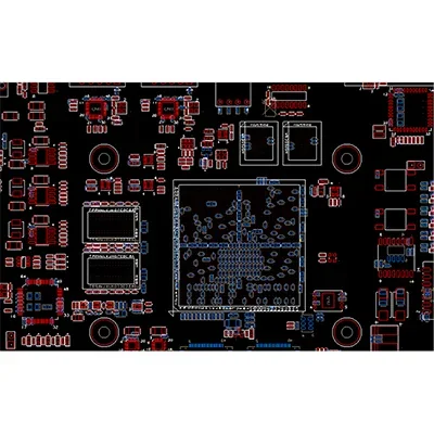
Hybrid high-frequency construction
The hybrid construction divides the substrate into a high-frequency area and an auxiliary area. The stack includes the substrate, internal and external circuit layers, and solder-mask layers.
The auxiliary area provides mechanical support, while the high-frequency inlay is fixed in its designated position. The high-frequency region can be formed independently, using high-frequency material only where the RF signal requires it.
This arrangement limits the amount of specialist high-frequency laminate while meeting signal requirements, helping reduce fabrication cost.
Hybrid-board design data
| Parameter | Design data |
|---|---|
| Layers | 6 |
| Materials | RO4350B + FR4 |
| Board thickness | 1.6 mm |
| Board size | 210 × 280 mm |
| Surface finish | Gold plating |
| Minimum hole diameter | 0.25 mm |
| Application | Communications |
| Construction characteristic | Hybrid high-frequency lamination |
Design and manufacturing capabilities
| Capability | Service range or option |
|---|---|
| Material options | TG170 / TG180, F4BM, FR4, FR1–4 and related materials |
| Design layer range | 1–32 layers |
| Minimum conductor width / spacing | 3 mil |
| Minimum laser-drilled hole | 4 mil |
| Minimum mechanically drilled hole | 8 mil |
| Copper foil thickness | 18–175 µm; standard values: 18, 35 and 70 µm |
| Peel strength | 1.25 N/mm |
| Minimum punched hole, single-sided board | 0.9 mm / 35 mil |
| Minimum hole diameter | 0.25 mm / 10 mil |
| Hole-diameter tolerance for holes ≤0.8 mm | ±0.05 mm |
| Hole-diameter tolerance | ±0.05 mm |
| Hole-wall copper, double-sided / multilayer | ≥0.8 mil |
| Via resistance, double-sided / multilayer | ≤300 µΩ |
| Minimum line width | 0.127 mm / 5 mil |
| Minimum line spacing | 0.127 mm / 5 mil |
| Silkscreen colors | Black, white, red, green and other colors |
| Surface finish options | Leaded / lead-free HASL, ENIG, silver and OSP |
| Service | OEM service |
| Standards and compliance references | ISO 9001, RoHS and UL |