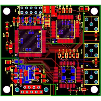
Circuit-board material and construction families
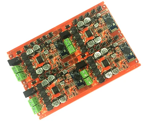
Circuit boards cover a wide range of constructions: ceramic boards, alumina ceramic boards, aluminum-nitride ceramic boards, aluminum-based boards, high-frequency boards, heavy-copper boards, impedance-controlled boards and ultra-thin boards. The familiar printed circuit board can also be described as a printed wiring board, including constructions formed by copper etching.
The board makes a circuit compact and easier to organize. It supports repeatable production of fixed circuits and the optimization of electrical layouts in electronic equipment.
Flexible printed circuits
A flexible printed circuit (FPC) uses a base such as polyimide or polyester film. This construction combines flexible routing with high wiring density, low weight, a thin profile and the ability to bend.
Combining rigid and flexible circuitry
The development of FPC and rigid PCB technology led to rigid-flex constructions. Flexible and rigid circuit sections are combined by lamination and related manufacturing processes to form a circuit board that incorporates the characteristics of both constructions.
Design and manufacturing capabilities
| Capability | Service range or option |
|---|---|
| Design layer range | 1–32 layers |
| Minimum conductor width / spacing | 3 mil |
| Minimum laser-drilled hole | 4 mil |
| Minimum mechanically drilled hole | 8 mil |
| Copper foil thickness | 18–175 µm; standard values: 18, 35 and 70 µm |
| Peel strength | 1.25 N/mm |
| Minimum punched hole, single-sided board | 0.9 mm / 35 mil |
| Minimum hole diameter | 0.25 mm / 10 mil |
| Hole-diameter tolerance for holes ≤0.8 mm | ±0.05 mm |
| Hole-diameter tolerance | ±0.05 mm |
| Hole-wall copper, double-sided / multilayer | ≥0.8 mil |
| Via resistance, double-sided / multilayer | ≤300 µΩ |
| Minimum line width | 0.127 mm / 5 mil |
| Minimum line spacing | 0.127 mm / 5 mil |
| Silkscreen colors | Black, white, red, green and other colors |
| Surface finish options | Leaded / lead-free HASL, ENIG, silver and OSP |
| Service | OEM service |
| Standards and compliance references | ISO 9001, RoHS and UL |