

















Via-in-Pad for BGA: How to Choose the Structure and Avoid Soldering Problems
You can place a via in a BGA solder pad when the routing and finished pad construction support it. The important question is what the solder ball will land on. An exposed hole can draw solder away; a properly finished plated-over pad provides a continuous solderable surface. Blind microvias need their own package and process review.
Via-in-pad can help you escape a crowded ball grid, but ball pitch alone doesn’t settle the choice. The land pattern, layer connections, available routing channels, and assembly process all matter.
This guide separates those decisions, explains what happens during printing and reflow, and shows how to interpret the evidence afterward. It focuses on BGA solder lands. Guidelines for a large exposed thermal pad should not be applied automatically to each individual BGA ball.
Does this BGA actually need via-in-pad?
Start with the package land pattern and the routes that must leave it. Work out whether a via needs to sit inside a solder land to reach the required copper layers. Check the ball map, escape direction, available routing layers, and nearby components before choosing the structure.
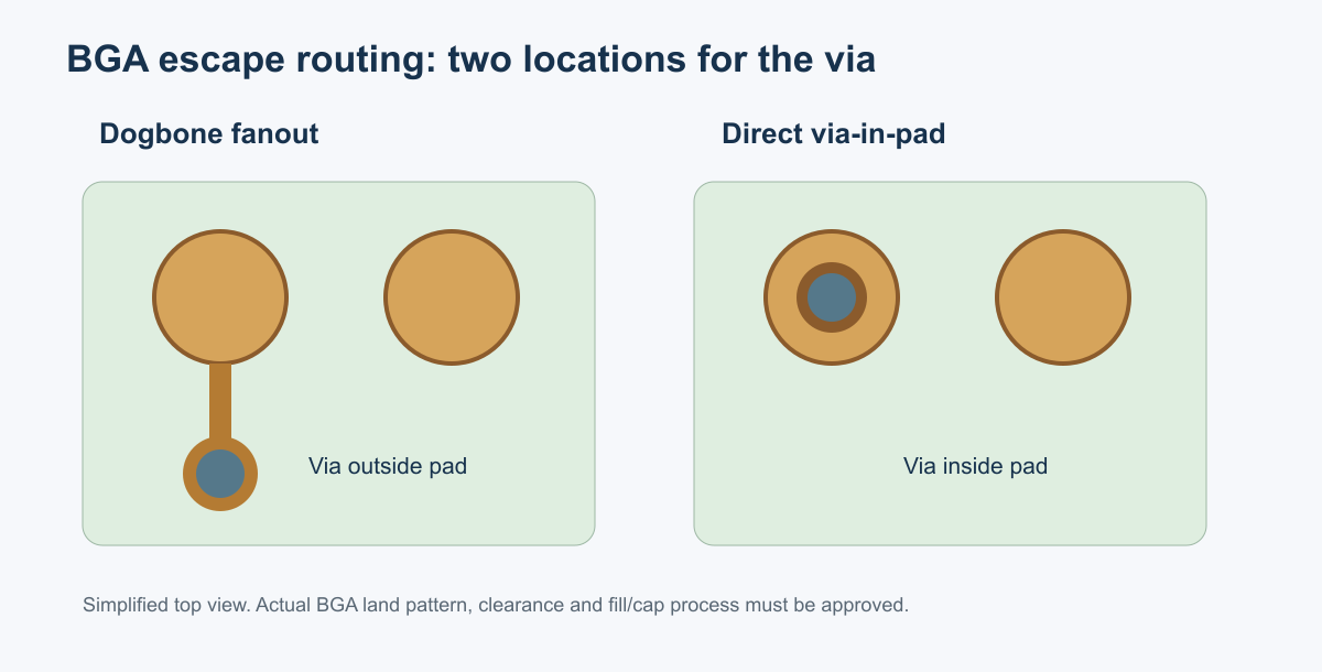
Illustration: Schematic fanout choices. The drawing compares the via’s position relative to the solder land; it does not specify scale, layer span, or manufacturing tolerances.
Start with the land pattern and escape path
Mark which balls need to connect to each layer, then trace the first segment of each escape route. A signal ball may have a clear path between neighboring lands, while a power or ground ball may need a connection to a nearby plane. The ball map tells you which routing problems actually exist.
Look at the land diameter and spacing, neighboring via clearances, trace width and spacing rules, and the direction each net must travel. Include the escape layer and the layers available for onward routing. An offset via can work if the connecting trace fits between adjacent features without blocking another essential route.
Use the package’s recommended land pattern and the board’s approved fabrication rules. Two packages at the same pitch can have different lands, missing-ball patterns, and routing constraints. Shrinking a solder land simply to make the fanout fit changes the assembly interface; it needs a separate review.
Dogbone, through-via, or blind microvia?
Dogbone describes a surface arrangement: a short trace leaves the solder land and reaches a nearby via. Via-in-pad describes the via’s position within the land. Through and blind describe which board layers the via connects. These are independent choices. A via in a pad can be through or blind; an offset via can also connect different layer ranges.
If a dogbone fits and reaches the intended layer, it may avoid additional pad treatment. If the connecting trace and via land consume space the escape needs, consider moving the via into the solder land. Choose its span from the required layer connections.
A through-via can reach deeper layers, but unused barrel length may create an electrical stub. A blind microvia reaches selected layers near the surface and requires a compatible stackup and fabrication process. Filling the opening doesn’t change which layers the via connects.
For high-speed nets, evaluate the transition as part of the complete signal path. Altera’s AN 875 discusses the effects of stubs, pad and drill geometry, antipads, and reference planes. FLJPCB’s high-speed via and back-drilling guide explores that separate electrical question.
The via location doesn’t tell you what the solder pad looks like
A drawing that shows a via centered in a BGA land tells you where the connection sits. It still needs to define the component-facing surface. An open hole, a mask cover, a plug, and a plated-over land present different conditions to the assembly process.
Open, tented, plugged, filled, and capped are different outcomes
An open via leaves the barrel opening exposed. A tented via has solder mask covering its opening; the mask doesn’t fill the barrel. A plugged via has material closing the opening, but that term alone doesn’t establish the depth of the plug or a copper-covered surface. A filled via contains fill material, yet filling alone doesn’t finish the solder land.
Terminology can vary between fabrication documents. Identify the actual material and finished surface rather than relying on one word.
| Construction | Surface at the opening | What remains to be established |
|---|---|---|
| Open | Exposed hole | Whether this package and process permit it |
| Tented | Solder mask cover | Coverage, location, and suitability; it isn’t a copper cap |
| Plugged | Plugging material | Plug extent and final surface treatment |
| Filled | Fill material | Surface level and whether copper overplating is required |
| Filled, planarized, and copper capped | Prepared fill beneath copper | Finished surface and acceptance of the completed construction |
TI’s SPRABB3, section 20.5, distinguishes via coverings from filled-and-plated-over construction. This June 2010 report addresses particular 0.5 mm package-on-package processors. Its blind-via discussion also illustrates why every in-pad microvia should not automatically receive the same resin-fill instruction.
What planarization and copper capping add
Planarization levels the filled area. Copper capping creates copper across the prepared opening, allowing the solder land to extend over the via. The cap still needs the specified surface finish and acceptable surface condition.
The existing cross-section illustration shows this distinction: the open construction interrupts the solder land; the filled-and-capped construction places a copper surface above the fill. It doesn’t show every possible blind-microvia process.
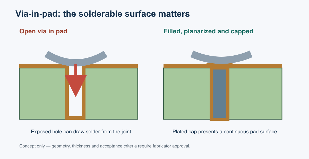
Illustration: Simplified cross-sections showing the opening, plated barrel, fill, and copper cap. Thicknesses and hole geometry are schematic, not production specifications.
NXP AN13656 recommends filled vias plated over to provide planar pads for its covered flip-chip BGA and CSP families. Apply the guidance for the actual component. The resin-filled via overview explains the fabrication sequence in more detail.
Why nonconductive fill can still make an electrical connection
In a resin-filled plated via, copper on the barrel connects the relevant copper layers. Nonconductive resin occupies the space inside that copper wall. The resin’s electrical insulation doesn’t disconnect the plated barrel.
The surface cap, barrel plating, and layer connections must still form the intended copper path. Specifying conductive fill cannot compensate for a missing connection or defective plating.
Keep thermal requirements separate too. A material selected to support a plated-over pad doesn’t, by that choice alone, establish heat-removal performance. Evaluate the copper path, via arrangement, stackup, and operating conditions when heat transfer is part of the design.
Follow the failure mechanism from printing to reflow
Different defects call for different investigations. An exposed via can allow solder drainage, while an uneven pad can disrupt printing. A void enclosed beneath an intact copper cap is another condition; it doesn’t by itself provide a passage from the solder joint into the barrel.
Solder drainage changes the joint’s solder supply
When molten solder wets an exposed plated via opening, some can move into the barrel. That leaves less solder available at the intended joint. The outcome depends on the opening, land geometry, paste deposit, and assembly process; an exposed via doesn’t mean every joint will fail.
NXP’s assembly guidance identifies inconsistent joints and voiding as risks of fully or partially open in-pad vias for the packages it covers. That supports examining the solder path, rather than treating an open hole as an ordinary uninterrupted land.
Distinguish two observations during diagnosis. Solder entering an exposed via concerns a pathway from the joint. A cavity inside fill under a continuous cap concerns the fabricated structure. If there’s no opening through the cap, that cavity isn’t evidence of direct solder drainage.
This distinction prevents the wrong correction. Increasing paste to compensate for one suspected mechanism can affect neighboring joints and bridging risk. Establish whether the pad is actually open before changing the process.
Recessed or uneven pads complicate paste deposition
A dish in the cap or local surface-height variation can change stencil contact and paste release. The deposit may differ from its intended volume or shape even with an unchanged stencil.
Infineon’s board assembly recommendations discuss pad planarity, via openings, and interactions with solder deposition and void formation. Its thermal-pad examples have a different geometry from individual BGA lands, so their stencil layouts aren’t interchangeable.
Keep the board surface, package terminals, and paste measurements separate. Pad planarity describes the land. Package coplanarity describes the relative position of the component’s terminals. Paste data describes the deposit after printing. A low paste reading alone doesn’t identify which condition caused it.
Look for a spatial pattern. Do unusual deposits coincide with the in-pad locations, occur across the whole footprint, or repeat elsewhere on the panel? Those comparisons guide the investigation; they don’t prove the cause. The SPI measurement guide explains the deposit measurements.
A larger aperture or hotter reflow profile isn’t a substitute for resolving an unacceptable pad surface. Each change needs evidence that it addresses the observed problem.
Mixed pad constructions need a package-specific review
Different constructions can respond differently to heating and cooling within one footprint. AMD’s DS955 BGA design rules advise against mixing PCB-pad-isolated VIPPO and non-VIPPO styles because localized z-direction expansion mismatch can cause hot-tear defects.
That warning applies to the designs addressed by the document. It isn’t a universal ban on every mixed BGA fanout. For your package, review which pads use each construction and what the component manufacturer’s guidance allows.
A successful first reflow also doesn’t establish rework robustness. Component removal and replacement introduce another thermal and handling sequence. Evaluate that sequence if rework is part of the product plan, especially when the pad construction or surrounding materials have changed.
What inspection can prove—and what it can’t
Choose evidence for the question you’re trying to answer. A bare-board construction check, an assembled-joint image, and an electrical test examine different parts of the problem. Combining them is useful when you understand the limits of each.
Bare-board evidence: surface and cross-section
Before assembly, examine the finished BGA lands for the specified surface condition. Optical inspection can identify visible openings or surface irregularities. If a dimensional planarity requirement applies, a photograph alone doesn’t demonstrate that it was met; use the agreed measurement method.
A microsection exposes the construction at the cut location. It can show the fill, copper cap, barrel, and connections intersected by that section. Interpretation depends on where the section passes through the feature.
Tie the sample or coupon to the relevant via construction and production lot. A coupon built with a different layer sequence may answer a different question. One acceptable section establishes evidence for that sample; the sampling plan determines how it supports the lot decision.
Assembly evidence: paste, X-ray, and electrical checks
SPI evaluates the paste before placement. It can reveal unusual deposits at particular pad locations, but it can’t verify the material beneath a copper cap.
After reflow, X-ray can help examine hidden solder geometry and visible voiding. Matsusada’s BGA inspection explanation shows why this view is useful under the package. The BGA X-ray guide discusses interpretation limits in more detail.
Don’t assign a fill defect from a joint image alone. The image, bare-board evidence, and observed failure need to agree before you name the mechanism.
Electrical checks establish behavior within their coverage and test conditions. A bare-board continuity test addresses the board network; an assembled functional test exercises selected circuits and operating states. Neither gives a direct measurement of every joint’s mechanical strength.
A passing check is not a lifetime guarantee
Inspection and initial operation don’t reproduce the product’s full service life. Qualification needs to address the relevant thermal and mechanical exposures when those are part of the reliability requirement.
NXP describes daisy-chain samples as a means of evaluating board-level solder-joint reliability. That is a qualification approach, not a promise that a particular sample is currently available or represents your assembly.
For an actual product, decide which construction and assembly process the qualification represents. Record changes that could invalidate that connection. This keeps a passing result attached to the design it evaluated.
Choose the simplest structure that meets the actual design
Start with the routing connection you need, then evaluate the pad surface that makes it assemble reliably. This produces a more useful comparison than selecting via-in-pad everywhere for convenience.
Compare routing benefit with the added fabrication process
A dogbone that satisfies the land pattern and routing constraints may avoid fill and cap processing. A plated-over in-pad via may free enough space to make an otherwise blocked escape practical. A blind-microvia route may change the required stackup and build sequence.
Compare complete alternatives. Include routing-layer needs, drilling, filling, planarization, copper capping, and any sequential build steps that each option actually requires. Don’t assume one additional process always costs less than another layer, or that changing the via style guarantees a layer reduction.
The benefit must appear in the layout: an accessible inner row, a workable plane connection, or a transition that meets the electrical requirement. If the proposed change doesn’t solve a defined constraint, reconsider why it is being added.
Recheck the choice when the stackup or package changes
A layer change can alter the via span. A new package revision can change the land pattern or ball map. A different fabrication process can change the finished pad condition. An apparently small change may therefore affect both routing and assembly.
Revisit the decision at those boundaries. Preserve the connection between the approved footprint, via construction, and assembly process rather than carrying forward an old label.
A workable BGA via-in-pad design joins three things: the required layer connection, a suitable solder land, and evidence that addresses the actual risks. Choose the simplest construction that achieves all three.