PCB Cleanliness Standards for Medical Electronics
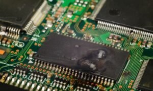
Cleanliness is not only for devices used in medicine. In fact, avoiding things like ionic contamination during the manufacture and assembly of circuit boards for medical electronic devices…
 FLJ PCBManufacturing your next idea
FLJ resources
Practical guides to PCB design, materials, manufacturing and assembly. Explore the details that matter before your next build.
Showing 71–82 of 112 articles
Cleanliness is not only for devices used in medicine. In fact, avoiding things like ionic contamination during the manufacture and assembly of circuit boards for medical electronic devices…
A trace impedance target does not automatically define the impedance of a via transition. A via is a three-dimensional discontinuity involving a plated barrel, pads, antipads, reference planes,…
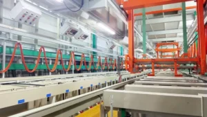
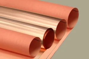
Sulfuric acid copper plating plays a very important role in PCB electroplating. The quality of acid copper plating directly affects the copper layer quality on the PCB. It…
FPC Circuit Design — Common Problems I. Overlap of Pads II. Misuse of Graphic Layers III. Random Placement of Silkscreen Text IV. Hole Size Setting for Single-side Pads…
PCB acts as the carrier for many components and as the hub for circuit signal transfer. It has become a very important and key part of electronic information…
When we analyze procurement costs using a procurement cost index and by looking at related commodity prices, the main goal is to see, at the company level, whether…
Electronics makers use multilayer printed circuit boards (PCBs) to make circuits take less space. This lets them put more parts on the top side of the board, and…
Abstract This paper explains the classification, material choice, technology trends, design rules, and processing standards for printed circuit boards (PCBs) used in communication products. It is for PCB…
HDI boards meet the needs of high density ICs and high density interconnect assembly. They push PCB manufacturing to a new level. HDI is one of the hottest…
Basic Process for Making HDI Boards with Blind and Buried Vias 1. Overview HDI stands for High Density Interconnect. It is a PCB technology that rose in the…
1. Core Principles of Stackup Design Overall, stackup design must follow two rules: Below are example stackups from two-layer boards up to eight-layer boards. 2. Stackup Schemes by…
In PCBs, many things can cause EMI. For example: radio frequency currents, common-mode voltages, ground loops, impedance mismatch, and magnetic flux. To control EMI, we need to learn…