
LED lighting has transformed from a niche technology into a $70+ billion global industry, with circuit boards serving as the critical backbone of every luminaire. PCBA manufacturing for LED applications demands precision engineering that balances thermal management, electrical performance, and cost efficiency—challenges that traditional electronics assembly rarely encounters at this scale.
The printed circuit board assembly process for LED products differs fundamentally from conventional electronics. LEDs generate heat in compact spaces. Compare standard FR-4 materials with aluminum- or copper-core constructions by reviewing the complete thermal path: dielectric thickness, copper layout, metal base and heatsink interface. According to Printed Circuit Board Assembly Market research, the global PCBA market is experiencing accelerated growth driven largely by LED adoption across automotive, architectural, and industrial sectors.
Modern LED PCBA integrates multiple disciplines: SMT component placement for driver ICs and passive components, thermal interface material application, and increasingly, chip-on-board (COB) direct LED mounting. The LED manufacturing sector continues evolving toward higher lumen density and longer operational lifespans, pushing PCBA manufacturers to adopt advanced materials and quality control protocols.
Understanding the nuances of LED-specific assembly processes separates adequate production from excellence—a distinction that directly impacts product reliability and manufacturer reputation in this competitive landscape.
Key Components in LED PCBA Manufacturing
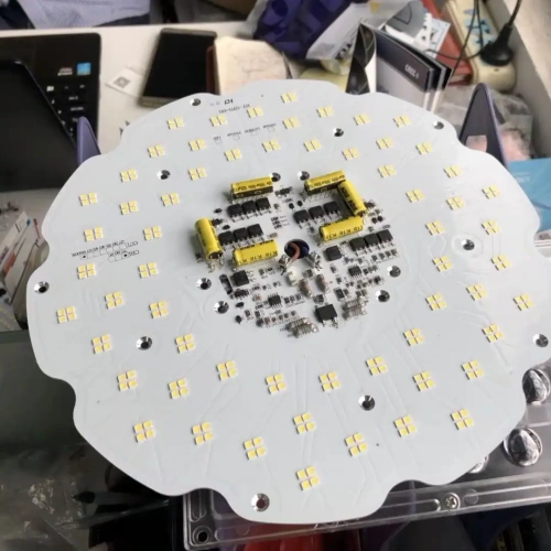
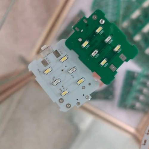
LED PCB manufacturing relies on several specialized components working in harmony to deliver reliable performance. At the foundation sits the substrate material—typically aluminum or copper-clad laminate—which provides thermal management capabilities critical for LED longevity. Compare dielectric thickness, base material and heatsink contact before choosing a substrate. For industry context, see the chip-on-board LED market overview.
The LED chips themselves represent the most critical component, with chip-on-board (COB) technology dominating modern designs. These chips mount directly onto the PCB, eliminating the need for individual LED packaging and improving heat dissipation. Surrounding the LEDs, current-limiting resistors and driver ICs regulate power delivery—a seemingly simple function that determines whether your LED fixture operates for 50,000 hours or fails prematurely.
Solder mask and silkscreen layers complete the assembly, protecting copper traces while identifying component positions during manufacturing. For basic single-layer designs, these components mount on one surface. However, complex LED systems increasingly use multilayer boards incorporating plated copper thermal vias that conduct heat toward copper planes or a heatsink. W/m·K describes a material property; an assembled thermal path must be assessed using its geometry and thermal resistance. This thermal architecture, invisible to end users, separates professional-grade LED lighting from consumer products that fade or flicker within months of installation.
Comparing PCBA Manufacturing Processes
Manufacturers employ three primary approaches to produce LED lighting PCB assemblies, each offering distinct advantages for different application requirements. Surface Mount Technology (SMT) dominates the industry, widely used in LED circuit board production due to its speed and precision. Through-Hole Technology (THT), while less common, provides superior mechanical stability for high-vibration environments like industrial fixtures. Chip-on-Board (COB) represents the most integrated approach, bonding LED dies directly to substrates for maximum thermal efficiency.
Selection criteria hinge on three factors: production volume, component density, and thermal management needs. SMT excels in high-volume scenarios where automation drives cost efficiency, while flexible PCB options enable unique form factors for architectural installations. COB technology shows the strongest growth trajectory, with the market projected to reach $4.8 billion by 2030 as manufacturers prioritize thermal performance.
However, no single method suits all applications. Street lighting often requires the durability of through-hole assembly, whereas consumer bulbs benefit from SMT’s miniaturization capabilities. The choice ultimately balances upfront tooling costs against long-term reliability requirements—a decision that shapes both manufacturing workflows and final product performance in today’s competitive lighting market.
Method One: Surface Mount Technology (SMT)
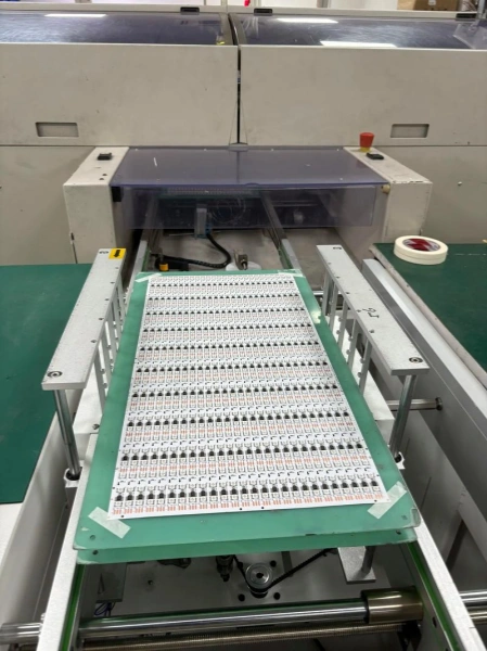
Surface Mount Technology dominates modern LED PCB assembly, accounting for the majority of commercial production due to its speed and component density advantages. This process mounts components directly onto the board’s surface rather than inserting leads through holes, enabling manufacturers to place thousands of components per hour using automated pick-and-place machines.
The SMT workflow begins with solder paste application through stencils, precisely depositing tin-based alloy onto copper pads. Automated placement machines then position LED chips, resistors, and driver ICs with accuracy down to 0.02mm—critical for maintaining uniform light output across arrays. Reflow ovens complete the process by melting solder paste in controlled temperature profiles, typically reaching 230-250°C for lead-free assemblies.
This approach excels for high-volume LED lighting production where cost per unit matters most. According to Printed Circuit Board Assembly Market analysis, SMT supports miniaturization and automated placement; a cost comparison requires the same BOM, volume, tooling and inspection scope. The modern assembly process achieves component placements that would be impossible manually.
However, SMT creates thermal management challenges. Components mounted flush against the board have limited heat dissipation pathways, requiring careful thermal design—particularly for high-power LED applications where junction temperatures directly impact lifespan and performance.
Method Two: Through-Hole Technology
Through-hole technology remains relevant for specific LED lighting applications despite SMT’s dominance in modern PCB fabrication for LED systems. This traditional assembly method inserts component leads through drilled holes in the board before soldering them on the opposite side, creating exceptionally robust mechanical bonds.
High-power LED fixtures—particularly those in industrial environments, outdoor streetlights, and automotive applications—frequently rely on through-hole components for critical connections. The process excels when assemblies must withstand sustained vibration, thermal cycling, or physical stress that might compromise surface-mounted joints. Power supplies, transformers, and heat-dissipating components in LED drivers often utilize this approach specifically for its enhanced reliability under mechanical stress.
However, through-hole assembly introduces notable limitations. Manufacturing speed decreases significantly compared to automated SMT lines, and component density remains constrained by hole spacing requirements. Labor costs typically run higher since manual insertion often supplements automated processes. Most contemporary LED PCBAs adopt a hybrid strategy—employing through-hole technology exclusively for high-stress connections while relying on SMT for the majority of components. This combination balances mechanical reliability with manufacturing efficiency, particularly in applications where failure carries safety or financial consequences.
LED PCBA Process Review Checklist
When an LED assembly shows premature failures, review the thermal path and assembly process before changing the production design. For SMT assembly LED products, record the failed units, operating conditions and failure symptoms so that a suspected cause can be tested.
Check the substrate construction and dielectric thermal resistance, the LED thermal-pad connection, heatsink contact, solder-joint condition and the measured reflow profile. Choose inspection stages and temperature limits from the component specifications and the approved process.
Verify the effect of each process change. Compare prototype thermal measurements, solder inspection and functional-test records under the same operating conditions. Track rework causes and repeat the agreed checks after the change. For industry context, see the Printed Circuit Board Assembly Market overview.
Agree the acceptance criteria before a trial build, document the revised process and retain the inspection and test records. Build the implementation budget from quotations for equipment, fixtures, process validation and operator training, and compare these costs with the expected production volume.
Technical Deep Dive: Thermal Management in LED PCBA
Effective thermal management represents the single most critical factor determining LED longevity and performance. While LEDs convert energy more efficiently than traditional lighting, approximately 65-80% of input power still dissipates as heat. Without proper thermal control, junction temperatures can exceed 150°C, dramatically accelerating lumen degradation and reducing operational lifespans by 50% or more.
LED chip mounting techniques directly influence thermal pathways. Direct thermal paths from the LED junction to the PCB substrate minimize thermal resistance—the primary barrier to heat dissipation. For metal-core PCBs (MCPCBs), distinguish the thermal conductivity of the dielectric from that of the metal base and the thermal resistance of the complete stack. The dielectric thickness, contact area and interface to the heatsink affect the result. However, advanced mounting techniques matter as much as substrate choice.
Thermal vias can conduct heat through an FR-4 stack toward copper planes or a heatsink. Select hole size, pad size, pitch and count from the LED package guidance, fabrication clearances and thermal analysis. Vias placed in solderable thermal pads may require filling and capping to control solder loss. Verify the resulting temperature rise on a prototype; via count or solder-paste thickness alone does not guarantee a junction-to-board thermal resistance.
The Printed Circuit Board Assembly Market increasingly demands thermal simulation during design phases. Computational fluid dynamics (CFD) modeling predicts hotspot formation before prototyping, so that candidate thermal paths can be compared before hardware is built. This preventive approach addresses thermal management at the architectural level rather than treating it as an afterthought.
Limitations and Considerations in LED PCBA
Despite the technological advancements in LED PCBA manufacturing, several inherent limitations require careful consideration during design and implementation. Understanding these constraints helps engineers make informed decisions and set realistic expectations for system performance.
Cost remains a significant barrier for widespread adoption. While LED technology has become more affordable, high-quality PCBA manufacturing—particularly for applications requiring advanced thermal management solutions—still commands premium pricing. The Chip-on-Board LED market reflects this reality, with advanced packaging configurations adding 15-30% to total production costs compared to conventional mounting techniques.
Design complexity introduces multiple failure points. The integration of power management circuits, driver electronics, and LED arrays on a single board creates interdependencies that can complicate troubleshooting. A single cold solder joint or inadequate thermal interface can cascade into system-wide performance degradation. The miniaturization trend exacerbates this challenge, as tighter component spacing increases susceptibility to thermal crosstalk and electromagnetic interference.
Material selection presents ongoing trade-offs between performance and cost. While metal-core PCBs offer superior heat dissipation, through-hole parts and multilayer routing need an appropriate insulated construction and fabricator review. A metal core does not categorically rule out through-hole components. Standard FR-4 substrates remain cost-effective but require more aggressive thermal management strategies, including larger heat sinks and forced air cooling—solutions that increase bill-of-materials costs and system complexity.
Key Takeaways
LED PCBA manufacturing stands at the intersection of precision electronics and thermal engineering, where material selection, assembly techniques, and thermal management collectively determine product longevity and performance. The industry’s trajectory toward miniaturization and higher power densities demands increasingly sophisticated approaches to heat dissipation, with aluminum substrates and advanced dielectric materials becoming standard rather than exceptional.
The global PCBA market’s projected growth to $11.6 billion by 2032 reflects not merely increased demand but a fundamental shift toward intelligent lighting systems that require more complex circuit integration. Success in this landscape requires manufacturers to balance competing priorities: thermal performance against cost constraints, automation against flexibility, and standardization against customization.
For manufacturers entering or expanding in LED PCBA production, three priorities emerge as non-negotiable: establishing robust thermal management protocols, implementing rigorous quality control at the component level, and maintaining flexibility to accommodate rapid technological evolution. The manufacturers who thrive will be those who view thermal management not as a technical challenge to solve but as a continuous optimization process that adapts to emerging LED chemistries, driver technologies, and application-specific requirements.
The future belongs to manufacturers who recognize that superior LED PCBA isn’t about individual excellence in assembly or design—it’s about systematic integration of materials science, thermal physics, and manufacturing precision.