
Usually, the thickness of a finished standard PCB is between 0.8 mm and 1.6 mm. The most common default board thickness is 1.6 mm (about 63 mil). Many connector standards are also designed for this 1.6 mm size. So how did this thickness standard come about?
The early stage of the PCB industry
From the history of PCB development, we can see that in the vacuum tube era, the PCB industry was still at an early stage. Because vacuum tubes gave off a lot of heat, they were large and not easy to mount on a printed board. They also needed a certain level of mechanical strength. At that time, electronic products were mostly built by hand.
In PCB base materials, this also had to do with the development of epoxy resins for PCB substrates. At that time, PCB base materials, copper foil, and other related manufacturing processes had not yet reached industrial production.
In the 1920s, circuit designers made boards from bakelite (phenolic resin), gypsum board, cardboard, and even thin wood sheets. These boards looked similar to circuit boards or breadboards. They drilled holes in the material, then used rivets or bolts to attach flat copper wires to the board and form an interconnect circuit.
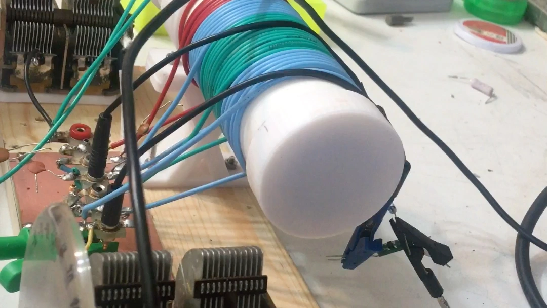
In the 1920s, the TRF radio made by Signal was built with a wooden breadboard.
The rise and spread of phenolic resin
Among these resins, bakelite was first synthesized in 1872 by the German chemist Adolf von Baeyer (1835–1917). In 1907, the American chemist Leo Hendrik Baekeland (1863–1944) improved the production process of phenolic resin and made it practical and industrially usable. In 1910, he founded the General Bakelite Company and named this material “Bakelite.”
In the early 20th century, based on Baekeland’s phenolic resin, industrial production of phenolic resin was started in Germany, the UK, France, Japan, and other countries. Phenolic resin also began to be widely used in radio knobs, turntables, circuit boards (not printed circuit boards), and product housings.
Phenolic laminate pushed PCB development forward
In 1927, laminate made by Formica was used in home radios and marine radios. In the same year, Formica found a way to add decorative paper by using a lithographic process, so the laminate could be made with wood grain and marble patterns. As laminate became more colorful and more decorative, many workbenches also used phenolic laminate as a surface material.
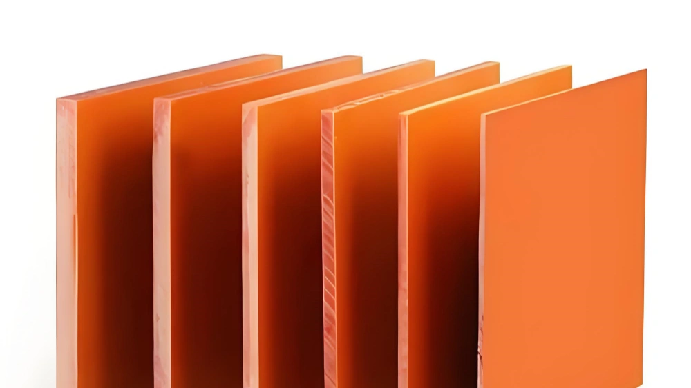
Phenolic laminate is a strong polymer material with good insulation. It also has heat resistance, water resistance, chemical resistance, and the ability to carry a relatively large current. Even though it was not made for circuit boards at first, its mechanical strength was much better than gypsum board, cardboard, and thin wood boards. So it slowly became an important base material for electronic circuit boards.
But on phenolic laminate, drilling holes and connecting all the electronic parts was still very hard, and it was even more troublesome than using a breadboard. Later, people invented a method of attaching copper foil to the surface of phenolic laminate and etching the trace pattern. In 1913, the British inventor Bury developed a process that coated a metal foil with an anti-etching resist and then formed conductive patterns by etching. This is seen as an important base of modern PCB manufacturing.
As the need for board interconnection kept growing, board connectors also appeared.
How the 1.6 mm board thickness standard formed
At that time, phenolic resin laminate was widely used in a thickness of 1/16 inch (about 63 mil, or 1.6 mm). So early board-to-board connectors, slots, and related products were also designed around 1/16 inch board thickness.
As the supply chain kept improving, a complete standard system formed around 1/16 inch (about 1.6 mm). Even after PCB materials and manufacturing processes changed greatly, 1.6 mm board thickness was still kept and slowly became the default standard thickness in the PCB industry.
Modern PCB board thickness standards
Today, substrate materials are much more diverse, but 1.6 mm (or 63 mil) is still the default finished board
thickness used by many PCB factories. The standard thickness range has also expanded to 0.8 mm to 1.6 mm.
(Please follow the board factory’s own standard. Some factories use 0.6 mm to 2.5 mm.)
If you need to make thinner or thicker PCBs, such as 0.4 mm or 3.0 mm boards (for example, 20-layer boards), extra material cost will be needed. So this must be considered in PCB design.
PCB copper thickness and current carrying capacity
In PCB fabrication, copper weight is commonly expressed in ounces per square foot. A copper weight of 1 oz/ft² corresponds to a nominal foil thickness of about 35 μm, not one ounce per square inch. Finished copper thickness can also be affected by plating, so specify the required finished thickness and tolerance with the fabricator.
Board thickness and copper thickness describe different dimensions. A 1.6 mm finished board can use different copper weights depending on its stack-up and electrical requirements.
How to evaluate trace width and current
There is no single current rating per millimetre of trace width. Required width depends on copper thickness, whether the trace is internal or external, the allowed temperature rise, ambient conditions, nearby copper, and the board stack-up. Use an appropriate method such as IPC-2152 together with the actual design conditions, and validate critical power paths rather than applying an unspecified current-density rule or universal derating percentage.
For an initial DC resistance estimate at approximately 20 °C, use:
Here R is resistance in ohms; copper resistivity ρ is approximately 0.0172 Ω·mm²/m; L is trace length in metres; and w and t are width and thickness in millimetres. For example, a 100 mm long, 1 mm wide trace with 35 μm copper has an estimated resistance of 0.049 Ω at 20 °C. This estimate excludes vias, connections, and manufacturing variation.
Resistive heating is P = I²R, and copper resistance rises with temperature. The resistance calculation alone does not establish a safe current rating. Confirm voltage drop and temperature rise for the finished layout, including neck-downs, vias, and connector transitions.